MJD3055 Overview
Description
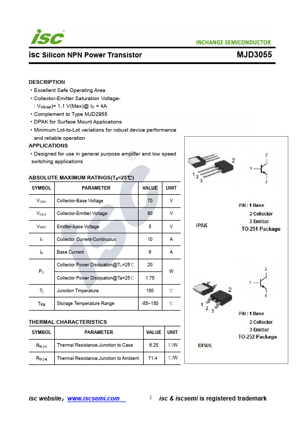
Excellent Safe Operating Area - Collector-Emitter Saturation Voltage- : VCE(sat)= 1.1 V(Max)@ IC = 4A - Complement to Type MJD2955 - DPAK for Surface Mount Applications - Minimum Lot-to-Lot variations for robust device performance and reliable operation APPLICATIONS - Designed for use in general purpose amplifer and low speed switching applications SYMBOL PARAMETER VALUE UNIT VCBO Collector-Base Voltage 70 V VCEO Collector-Emitter Voltage 60 V VEBO Emitter-base Voltage 5 V IC Collector Current-Continuous 10 A IB Base Current 6 A Collector Power Dissipation@TC=25℃ 20 PC W Collector Power Dissipation@Ta=25℃ 1.75 Tj Junction Tmperature 150 ℃ Tstg Storage Temperature Range -55~150 ℃ SYMBOL PARAMETER VALUE UNIT Rth j-c 6.25 ℃/W Rth j-a isc website: 1 isc & iscsemi is registered trademark isc Silicon NPN Power Transistors INCHANGE Semiconductor MJD3055 TC=25℃ unless otherwise specified SYMBOL PARAMETER CONDITIONS VCEO(SUS) Collector-Emitter Sustaining Voltage IC= 30mA ;IB= 0 VCE(sat)-1 Collector-Emitter Saturation Voltage IC= 4A ;IB= 0.4A VCE(sat)-2 Collector-Emitter Saturation Voltage IC= 10A ;IB= 3.3A VBE(on) Base-Emitter On Voltage IC= 4A ; VCE= 4V ICEO Collector Cutoff Current VCE= 30V; IB=0 ICBO Collector Cutoff Current VCB= 100V; IE=0 IEBO Emitter Cutoff Current VEB= 5V; IC= 0 hFE-1 DC Current Gain IC= 4A ; VCE= 4V hFE-2 DC Current Gain IC= 10A ; VCE= 4V fT Current-Gain-Bandwidth Product Pulse Test: PW≤300μs, Duty Cycle≤2.0% IC= 0.5A ; VCE= 10V;ftest= 1.0MHz MIN MAX UNIT 60 V 1.1 V 8.0 V 1.8 V 50 uA 0.02 mA 0.5 mA 20 100 5 2.0 MHz isc website: 2 isc & iscsemi is registered.