Datasheet4U Logo Datasheet4U.com

THC63LVDF64B - (THC63LVDF64B / THC63LVDF84B) LVDS Color Host-LCD Panel Interface Receiver

Description

The THC63LVDF84B/THC63LVDF64B receiver supports wide VCC range(2.5~3.6V).

At single 2.5V supply, the THC63LVDF84B/THC63LVDF64B reduces EMI and power consumption.

Features

  • Wide VCC range: 2.5~3.6V.
  • Wide dot clock range: 20-85MHz suited for VGA,.
  • SVGA, XGA and SXGA (VCC=3.0~3.6V) Wide dot clock range: 20-70MHz suited for VGA, SVGA, XGA and SXGA (VCC=2.5V~3.6V).
  • PLL requires No external components.
  • Rx power consumption < 80mW @VCC 2.5V, 65MHz Grayscale.
  • Power-Down Mode.
  • Low profile 56 Lead or 48 Lead TSSOP Package.
  • Pin compatible with THC63LVDF84A/F64A Block Diagram THC63LVDF84B CMOS/TTL OU.

📥 Download Datasheet

Datasheet Details

Part number THC63LVDF64B
Manufacturer THine Electronics
File Size 197.88 KB
Description (THC63LVDF64B / THC63LVDF84B) LVDS Color Host-LCD Panel Interface Receiver
Datasheet download datasheet THC63LVDF64B Datasheet

Full PDF Text Transcription (Reference)

The following content is an automatically extracted verbatim text from the original manufacturer datasheet and is provided for reference purposes only.

View original datasheet text
www.DataSheet4U.com THC63LVDF84B/THC63LVDF64B_Rev2.0 THC63LVDF84B/THC63LVDF64B LVDS 24Bit/18Bit COLOR HOST-LCD PANEL INTERFACE RECEIVER
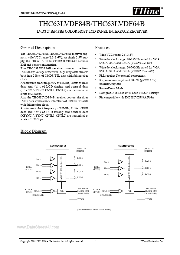
 General Description The THC63LVDF84B/THC63LVDF64B receiver supports wide VCC range(2.5~3.6V). At single 2.5V supply, the THC63LVDF84B/THC63LVDF64B reduces EMI and power consumption. The THC63LVDF84B receiver convert the four LVDS(Low Voltage Differential Signaling) data streams back into 28bits of CMOS/TTL data with falling edge clock. At a transmit clock frequency of 85MHz, 28bits of RGB data and 4bits of LCD timing and control data (HSYNC, VSYNC, CNTL1, CNTL2) are transmitted at a rate of 2.3Gbps. Also the THC63LVDF64B receiver convert the three LVDS data streams back into 21bits of CMOS/TTL data with falling edge clock.
Published: |