Datasheet4U Logo Datasheet4U.com

SSM6K403TU - Silicon N-Channel MOSFET

Key Features

  • (1) 1.5-V drive (2) Low drain-source on-resistance : RDS(ON) = 66 mΩ (max) (@VGS = 1.5 V) RDS(ON) = 43 mΩ (max) (@VGS = 1.8 V) RDS(ON) = 32 mΩ (max) (@VGS = 2.5 V) RDS(ON) = 28 mΩ (max) (@VGS = 4.0 V) 3. Packaging and Internal Circuit UF6 SSM6K403TU 1: Drain 2: Drain 3: Gate 4: Source 5: Drain 6; Drain ©2021-2022 1 Toshiba Electronic Devices & Storage Corporation Start of commercial production 2008-01 2022-02-02 Rev.1.0 SSM6K403TU 4. Absolute Maximum Ratings (Note) (Unless otherwise speci.

📥 Download Datasheet

Datasheet Details

Part number SSM6K403TU
Manufacturer Toshiba
File Size 428.70 KB
Description Silicon N-Channel MOSFET
Datasheet download datasheet SSM6K403TU Datasheet

Full PDF Text Transcription for SSM6K403TU (Reference)

Note: Below is a high-fidelity text extraction (approx. 800 characters) for SSM6K403TU. For precise diagrams, and layout, please refer to the original PDF.

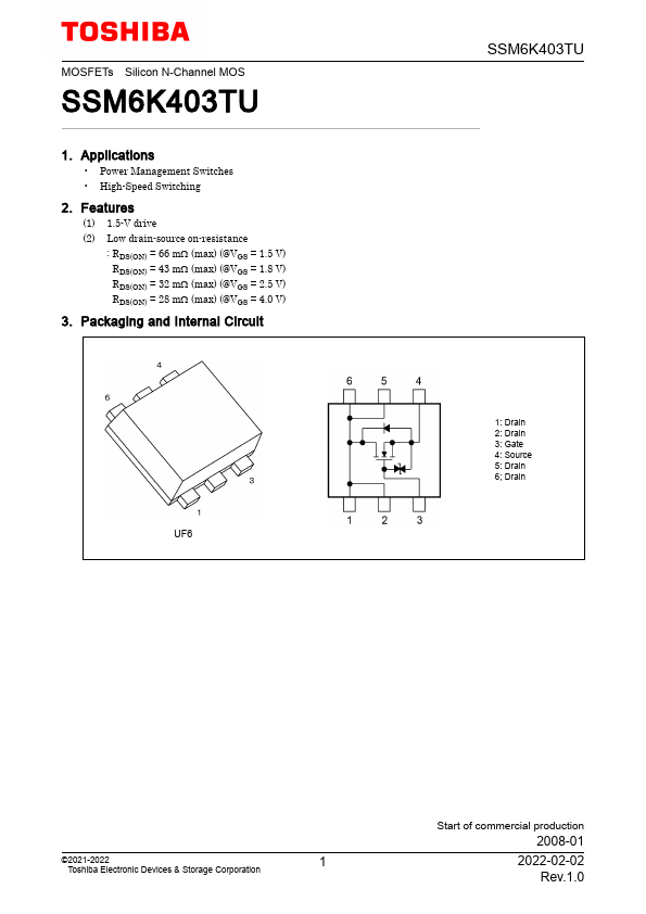
MOSFETs Silicon N-Channel MOS SSM6K403TU 1. Applications • Power Management Switches • High-Speed Switching 2. Features (1) 1.5-V drive (2) Low drain-source on-resistance...

View more extracted text
itching 2. Features (1) 1.5-V drive (2) Low drain-source on-resistance : RDS(ON) = 66 mΩ (max) (@VGS = 1.5 V) RDS(ON) = 43 mΩ (max) (@VGS = 1.8 V) RDS(ON) = 32 mΩ (max) (@VGS = 2.5 V) RDS(ON) = 28 mΩ (max) (@VGS = 4.0 V) 3. Packaging and Internal Circuit UF6 SSM6K403TU 1: Drain 2: Drain 3: Gate 4: Source 5: Drain 6; Drain ©2021-2022 1 Toshiba Electronic Devices & Storage Corporation Start of commercial production 2008-01 2022-02-02 Rev.1.0 SSM6K403TU 4. Absolute Maximum Ratings (Note) (Unless otherwise specified, Ta = 25 �) Characteristics Symbol Rating Unit Drain-source voltage Gate-source voltage VDSS 20 V VGSS ±10 Drain