Datasheet4U Logo Datasheet4U.com

SSM6N57NU - N-Channel MOSFET

Key Features

  • (1) 1.8 V gate drive voltage. (2) Low drain-source on-resistance : RDS(ON) = 39.1 mΩ (max) (@VGS = 4.5 V) RDS(ON) = 53 mΩ (max) (@VGS = 2.5 V) RDS(ON) = 82 mΩ (max) (@VGS = 1.8 V) 3. Packaging and Internal Circuit UDFN6 SSM6N57NU 1. Source1 (S1) 2. Gate1 (G1) 3. Drain2 (D2) 4. Source2 (S2) 5. Gate2 (G2) 6. Drain1 (D1) ©2019-2021 1 Toshiba Electronic Devices & Storage Corporation Start of commercial production 2012-07 2021-09-17 Rev.4.0 SSM6N57NU 4. Absolute Maximum Ratings (Note) (Unless o.

📥 Download Datasheet

Full PDF Text Transcription for SSM6N57NU (Reference)

Note: Below is a high-fidelity text extraction (approx. 800 characters) for SSM6N57NU. For precise diagrams, and layout, please refer to the original PDF.

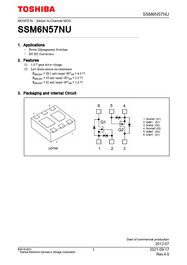
MOSFETs Silicon N-Channel MOS SSM6N57NU 1. Applications • Power Management Switches • DC-DC Converters 2. Features (1) 1.8 V gate drive voltage. (2) Low drain-source on-r...

View more extracted text
rs 2. Features (1) 1.8 V gate drive voltage. (2) Low drain-source on-resistance : RDS(ON) = 39.1 mΩ (max) (@VGS = 4.5 V) RDS(ON) = 53 mΩ (max) (@VGS = 2.5 V) RDS(ON) = 82 mΩ (max) (@VGS = 1.8 V) 3. Packaging and Internal Circuit UDFN6 SSM6N57NU 1. Source1 (S1) 2. Gate1 (G1) 3. Drain2 (D2) 4. Source2 (S2) 5. Gate2 (G2) 6. Drain1 (D1) ©2019-2021 1 Toshiba Electronic Devices & Storage Corporation Start of commercial production 2012-07 2021-09-17 Rev.4.0 SSM6N57NU 4.