SSM6N55NU
SSM6N55NU is N-Channel MOSFET manufactured by Toshiba.
MOSFETs Silicon N-Channel MOS
1. Applications
- Power Management Switches
- DC-DC Converters
2. Features
(1) 4.5V gate drive voltage. (2) Low drain-source on-resistance
: RDS(ON) = 46 mΩ (max) (@VGS = 10 V) RDS(ON) = 64 mΩ (max) (@VGS = 4.5 V)
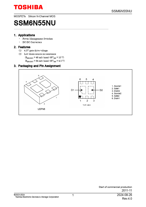
3. Packaging and Pin Assignment
UDFN6
1. Source1 2. Gate1 3. Drain2 4. Source2 5. Gate2 6. Drain1
©2023-2024
Toshiba Electronic Devices & Storage Corporation
Start of mercial production
2011-11
2024-08-26 Rev.4.0
4....