TH50VSF2581AASB
Overview
- Data retention supply voltage VCCs = 1.5 V~3.6 V
- Current consumption Operating: 45 mA maximum (CMOS level) Standby: 7 µA maximum (SRAM CMOS level) Standby: 10 µA maximum (flash CMOS level)
- Block erase architecture for flash memory 8 blocks of 8 Kbytes 63 blocks of 64 Kbytes
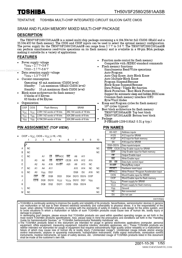
- Organization
- CIOF VCC VCC VSS CIOS VCC VSS VSS Flash Memory 2,097,152 words of 16 bits 2,097,152 words of 16 bits 4,194,304 words of 8 bits SRAM 262,144 words of 16 bits 524,288 words of 8 bits 524,288 words of 8 bits * * * *
- Function mode control for flash memory Compatible with JEDEC-standard commands Flash memory functions Simultaneous Read/Write operations Auto-Program Auto Chip Erase, Auto Block Erase Auto Multiple-Block Erase Program Suspend/Resume Block-Erase Suspend/Resume Data Polling / Toggle Bit function Block Protection / Boot Block Protection Support for automatic sleep and hidden ROM area Common flash memory interface (CFI) Byte/Word Modes Erase and Program cycles for flash memory 105 cycles (typical) Boot block architecture for flash memory TH50VSF2580AASB: Top boot block TH50VSF2581AASB: Bottom boot block Package P-FBGA69-1209-0.80A3: 0.31 g (typ.)