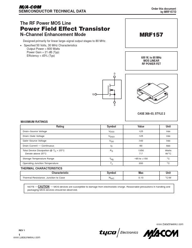
Datasheet4U Logo Datasheet4U.com

MRF157 - MOS LINEAR RF POWER FET

Features

  • r>.
  • to.
  • source threshold voltage, VGS(th). Cgd GATE Cgs DRAIN Ciss = Cgd + Cgs Coss = Cgd + Cds Crss = Cgd Cds SOURCE REV 1 5 Gate Voltage Rating.
  • Never exceed the gate voltage rating. Exceeding the rated VGS can result in permanent damage to the oxide layer in the gate region. Gate Termination.
  • The gates of these devices are essentially capacitors. Circuits that leave the gate open.
  • circuited or floating should be avoided. These conditions can result in.

📥 Download Datasheet

Full PDF Text Transcription (Reference)

The following content is an automatically extracted verbatim text from the original manufacturer datasheet and is provided for reference purposes only.

View original datasheet text
( DataSheet : www.DataSheet4U.com ) SEMICONDUCTOR TECHNICAL DATA Order this document by MRF157/D The RF Power MOS Line Power Field Effect Transistor N–Channel Enhancement Mode Designed primarily for linear large–signal output stages to 80 MHz. • Specified 50 Volts, 30 MHz Characteristics Output Power = 600 Watts Power Gain = 21 dB (Typ) Efficiency = 45% (Typ) MRF157 600 W, to 80 MHz MOS LINEAR RF POWER FET D G S CASE 368–03, STYLE 2 MAXIMUM RATINGS Rating Drain–Source Voltage Drain–Gate Voltage Gate–Source Voltage Drain Current — Continuous Total Device Dissipation @ TC = 25°C Derate above 25°C Storage Temperature Range Operating Junction Temperature Symbol VDSS VDGO VGS ID PD Tstg TJ Value 125 125 ±40 60 1350 7.
Published: |