www.vishay.com
VB30100S-M3
Vishay General Semiconductor
High-Voltage Trench MOS Barrier Schottky Rectifier
Ultra Low VF = 0.39 V at IF = 5 A
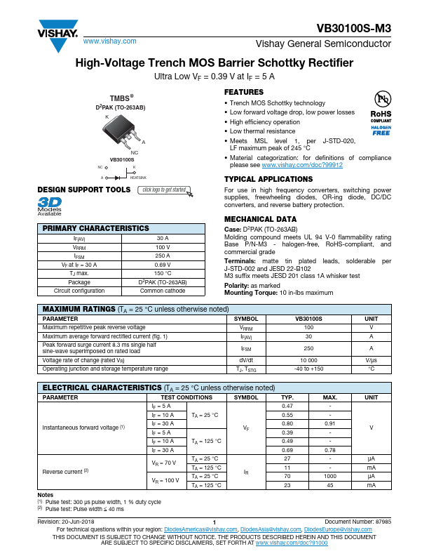
TMBS ®
D2PAK (TO-263AB)
K
A
NC
VB30100S
NC K
A HEATSINK
DESIGN SUPPORT TOOLS click logo to get started
Models
Available
PRIMARY CHARACTERISTICS
IF(AV)
VRRM
IFSM
VF at IF = 30 A
TJ max.
Package
30 A
100 V
250 A
0.69 V
150 °C
D2PAK (TO-263AB)
Circuit configuration
Common cathode
FEATURES
• Trench MOS Schottky technology
• Low forward voltage drop, low power losses
• High efficiency operation
• Low thermal resistance
• Meets MSL level 1, per J-STD-020,
LF maximum peak of 245 °C
• Material categorization: for definitions of compliance
please see www.vishay.com/doc?99912
TYPICAL APPLICATIONS
For use in high frequency converters, switching power
supplies, freewheeling diodes, OR-ing diode, DC/DC
converters, and reverse battery protection.
MECHANICAL DATA
Case: D2PAK (TO-263AB)
Molding compound meets UL 94 V-0 flammability rating
Base P/N-M3 - halogen-free, RoHS-compliant, and
commercial grade
Terminals: matte tin plated leads, solderable per
J-STD-002 and JESD 22-B102
M3 suffix meets JESD 201 class 1A whisker test
Polarity: as marked
Mounting Torque: 10 in-lbs maximum
MAXIMUM RATINGS (TA = 25 °C unless otherwise noted)
PARAMETER
SYMBOL
Maximum repetitive peak reverse voltage
Maximum average forward rectified current (fig. 1)
Peak forward surge current 8.3 ms single half
sine-wave superimposed on rated load
VRRM
IF(AV)
IFSM
Voltage rate of change (rated VR)
Operating junction and storage temperature range
dV/dt
TJ, TSTG
VB30100S
100
30
250
10 000
-40 to +150
UNIT
V
A
A
V/μs
°C
ELECTRICAL CHARACTERISTICS (TA = 25 °C unless otherwise noted)
PARAMETER
TEST CONDITIONS
SYMBOL
Instantaneous forward voltage (1)
Reverse current (2)
IF = 5 A
IF = 10 A
IF = 30 A
IF = 5 A
IF = 10 A
IF = 30 A
VR = 70 V
VR = 100 V
TA = 25 °C
TA = 125 °C
TA = 25 °C
TA = 125 °C
TA = 25 °C
TA = 125 °C
VF
IR
Notes
(1) Pulse test: 300 μs pulse width, 1 % duty cycle
(2) Pulse test: Pulse width 40 ms
TYP.
0.47
0.55
0.80
0.39
0.49
0.69
27
11
70
23
MAX.
-
-
0.91
-
-
0.78
-
-
1000
45
UNIT
V
μA
mA
μA
mA
Revision: 20-Jun-2018
1 Document Number: 87985
For technical questions within your region: DiodesAmericas@vishay.com, DiodesAsia@vishay.com, DiodesEurope@vishay.com
THIS DOCUMENT IS SUBJECT TO CHANGE WITHOUT NOTICE. THE PRODUCTS DESCRIBED HEREIN AND THIS DOCUMENT
ARE SUBJECT TO SPECIFIC DISCLAIMERS, SET FORTH AT www.vishay.com/doc?91000