www.vishay.com
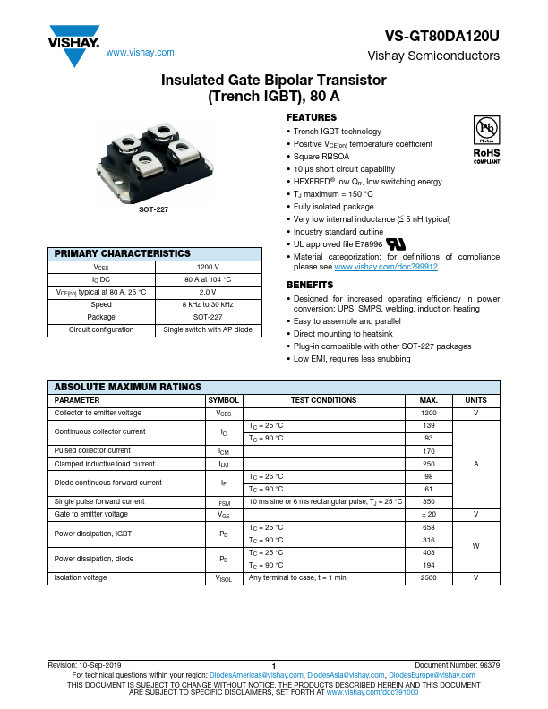
VS-GT80DA120U
Vishay Semiconductors
ELECTRICAL SPECIFICATIONS (TJ = 25 °C unless otherwise specified)
PARAMETER
SYMBOL
TEST CONDITIONS
Collector to emitter breakdown voltage
Collector to emitter voltage
Gate threshold voltage
Temperature coefficient of threshold voltage
Collector to emitter leakage current
Forward voltage drop
Gate to emitter leakage current
VBR(CES)
VCE(on)
VGE(th)
VGE(th)/TJ
ICES
VFM
IGES
VGE = 0 V, IC = 2.6 mA
VGE = 15 V, IC = 80 A
VGE = 15 V, IC = 80 A, TJ = 125 °C
VGE = 15 V, IC = 80 A, TJ = 150 °C
VCE = VGE, IC = 2.6 mA
VCE = VGE, IC = 2.6 mA (25 °C to 125 °C)
VGE = 0 V, VCE = 1200 V
VGE = 0 V, VCE = 1200 V, TJ = 125 °C
IF = 80 A, VGE = 0 V
IF = 80 A, VGE = 0 V, TJ = 125 °C
IF = 80 A, VGE = 0 V, TJ = 150 °C
VGE = ± 20 V
MIN.
1200
-
-
-
4.75
-
-
-
-
-
-
-
TYP.
-
2.0
2.4
2.5
5.7
-12
1.0
0.9
2.9
3.1
3.1
-
MAX.
-
2.55
-
-
7.0
-
100
-
3.5
-
-
± 220
UNITS
V
mV/°C
μA
mA
V
nA
SWITCHING CHARACTERISTICS (TJ = 25 °C unless otherwise specified)
PARAMETER
SYMBOL
TEST CONDITIONS
Total gate charge (turn-on)
Input capacitance
Reverse transfer capacitance
Turn-on switching loss
Turn-off switching loss
Total switching loss
Turn-on switching loss
Turn-off switching loss
Total switching loss
Turn-on delay time
Rise time
Turn-off delay time
Fall time
Reverse bias safe operating area
Qg
Cies
Cres
Eon
Eoff
Etot
Eon
Eoff
Etot
td(on)
tr
td(off)
tf
RBSOA
Diode reverse recovery time
Diode peak reverse current
Diode recovery charge
Diode reverse recovery time
Diode peak reverse current
Diode recovery charge
Short circuit safe operating area
trr
Irr
Qrr
trr
Irr
Qrr
SCSOA
VGE = -15 V, VGE = ± 15 V
VCE = 25 V, VGE = 0 V, f = 1 MHz
IC = 80 A, VCC = 600 V, VGE = 15 V,
Rg = 1.0 L = 500 μH,
TJ = 25 °C
IC = 80 A, VCC = 600 V, VGE = 15 V,
Rg = 1.0 L = 500 μH, TJ = 125 °C
Energy losses
include tail and
diode recovery
Diode used
HFA16PB120
TJ = 150 °C, IC = 250 A, Rg = 1.0 VGE = 15 V to 0 V,
VCC = 800 V, VP = 1200 V, L = 500 μH
IF = 50 A, dIF/dt = 200 A/μs, VR = 400 V
IF = 50 A, dIF/dt = 200 A/μs,
Vrr = 400 V, TJ = 125 °C
VGE = 15 V, VCC = 800 V, VCE max.= 1200 V, TJ = 150 °C
MIN.
-
-
-
-
-
-
-
-
-
-
-
-
-
TYP.
570
4400
235
3.0
3.2
6.2
3.9
5.5
9.4
134
65
281
155
MAX.
-
-
-
-
-
-
-
-
-
-
-
-
-
Fullsquare
- 179 -
- 11.5 -
- 1029 -
- 275 -
- 17.8 -
- 2451 -
10
UNITS
pF
mJ
mJ
ns
ns
A
nC
ns
A
nC
μs
THERMAL AND MECHANICAL SPECIFICATIONS
PARAMETER
SYMBOL
TEST CONDITIONS
MIN.
Junction and storage temperature range
Junction to case
IGBT
Diode
TJ, TStg
RthJC
-40
-
-
Case to heatsink
Weight
RthCS
Flat, greased surface
-
-
Mounting torque
Torque to terminal
Torque to heatsink
-
-
Case style
SOT-227
TYP.
-
-
-
0.1
30
-
-
MAX.
150
0.19
0.31
-
-
1.1 (9.7)
1.3 (11.5))
UNITS
°C
°C/W
g
Nm (lbf. in)
Nm (lbf. in)
Revision: 10-Sep-2019
2 Document Number: 96379
For technical questions within your region: DiodesAmericas@vishay.com, DiodesAsia@vishay.com, DiodesEurope@vishay.com
THIS DOCUMENT IS SUBJECT TO CHANGE WITHOUT NOTICE. THE PRODUCTS DESCRIBED HEREIN AND THIS DOCUMENT
ARE SUBJECT TO SPECIFIC DISCLAIMERS, SET FORTH AT www.vishay.com/doc?91000