S852TW
Overview
- Low supply voltage
- Low current consumption
- 50 W input impedance at 945 MHz 1
- Low noise figure
- High power gain 1
| Part | S852TW |
|---|---|
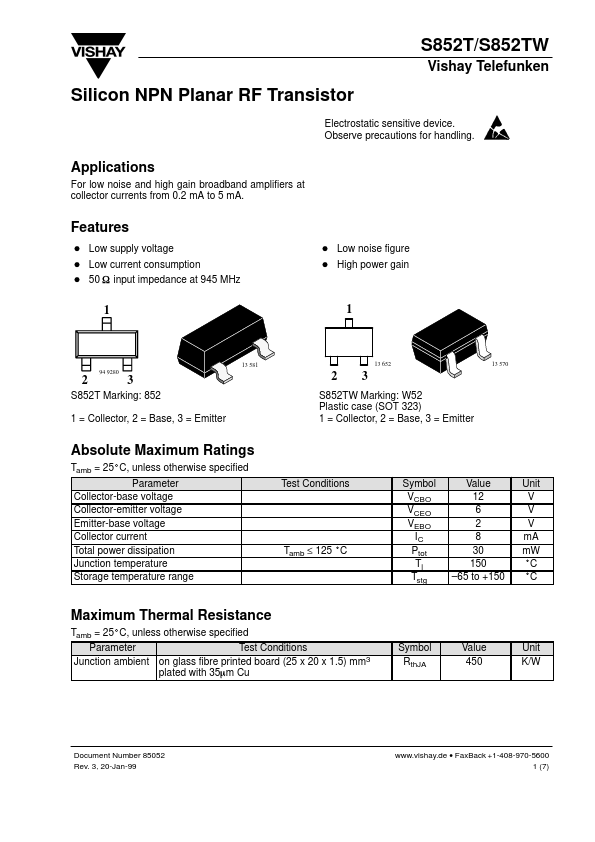
| Description | Silicon NPN Planar RF Transistor |
| Category | Transistor |
| Manufacturer | Vishay |
| Size | 119.82 KB |
| Part Number | Manufacturer | Description |
|---|---|---|
| S852TF | Vishay | Silicon NPN Planar RF Transistor |
| S8550 | Unisonic Technologies | LOW VOLTAGE HIGH CURRENT SMALL SIGNAL PNP TRANSISTOR |
| S8550 | Weitron Technology | PNP Transistor |
| S85N10R | SI-TECH | N-Channel MOSFET |
| S8550LT1 | Wing Shing Computer Components | HIGH VOLTAGE TRANSISTOR |