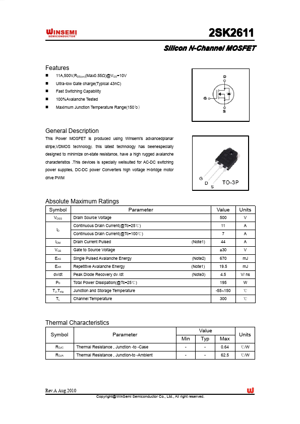
Datasheet4U Logo Datasheet4U.com

2SK2611 Datasheet Silicon N-Channel MOSFET

Manufacturer: WINSEMI SEMICONDUCTOR

Overview: www.DataSheet.in 2SK2611 Silicon N-Channel MOSFET.

Datasheet Details

Part number 2SK2611
Manufacturer WINSEMI SEMICONDUCTOR
File Size 538.17 KB
Description Silicon N-Channel MOSFET
Download 2SK2611 Download (PDF)

General Description

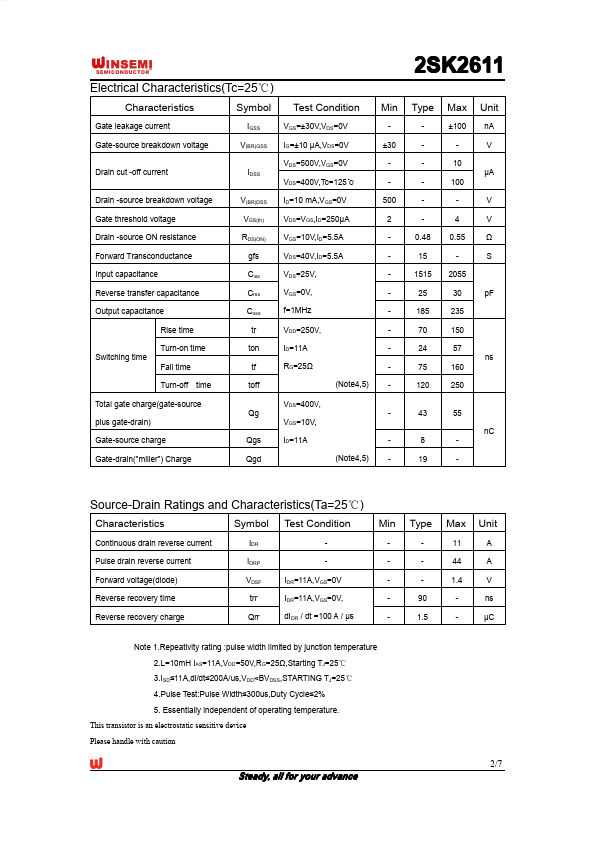
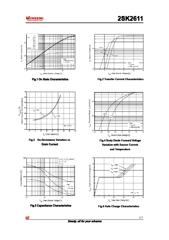
This Power MOSFET is produced using Winsemi's advancedplanar stripe,VDMOS technology.

this latest technology has beenespecially designed to minimize on-state resistance, have a high rugged avalanche characteristics .This devices is specially wellsuited for AC-DC switching power supplies, DC-DC power Converters high voltage H-bridge motor drive PWM Absolute Maximum Ratings Symbol VDSS ID IDM VGS EAS EAR dv/dt PD TJ,Tstg TL Drain Source Voltage Continuous Drain Current(@Tc=25℃) Continuous Drain Current(@Tc=100℃) Drain Current Pulsed Gate to Source Voltage Single Pulsed Avalanche Energy Repetitive Avalanche Energy Peak Diode Recovery dv /dt Total Power Dissipation(@Tc=25℃) Junction and Storage Temperature Channel Temperature (Note2) (Note1) (Note3) (Note1) Parameter Value 500 11 7 44 ±30 670 19.5 4.5 195 -55~150 300 Units V A A A V mJ mJ V/ ns W ℃ ℃ Thermal Characteristics Symbol RQJC RQJA Parameter Thermal Resistance , Junction -to -Case Thermal Resistance , Junction-to -Ambient Value Min - Typ - Max 0.64 62.5 Units ℃/W ℃/W Rev.A Aug.2010 Copyright@WinSemi Semiconductor Co., Ltd., All right reserved.

www.DataSheet.in 2SK2611 Electrical Characteristics(Tc=25℃) Characteristics Gate leakage current Gate-source breakdown voltage Symbol IGSS V(BR)GSS Test Condition VGS=±30V,VDS=0V IG=±10 µA,VDS=0V VDS=500V,VGS=0V Min ±30 500 2 - Type 0.48 15 1515 25 185 70 24 75 120 43 8 19 Max ±100 10 Unit nA V Drain cut -off current IDSS VDS=400V,Tc=125℃ 100 4 0.55 2055 30 235 150 57 µA Drain -source breakdown voltage Gate threshold voltage Drain -source ON resistance Forward Transconductance Input capacitance Reverse transfer capacitance Output capacitance Rise time Turn-on time Switching time Fall time Turn-off time T

Key Features

  • 11A,500V,RDS(on)(Max0.55Ω)@VGS=10V Ultra-low Gate charge(Typical 43nC) Fast Switching Capability 100%Avalanche Tested Maximum Junction Temperature Range(150℃) General.