YJL3416A
YJL3416A is N-Channel Enhancement Mode Field Effect Transistor manufactured by Yangjie Electronic.
Ro HS
PLIANT
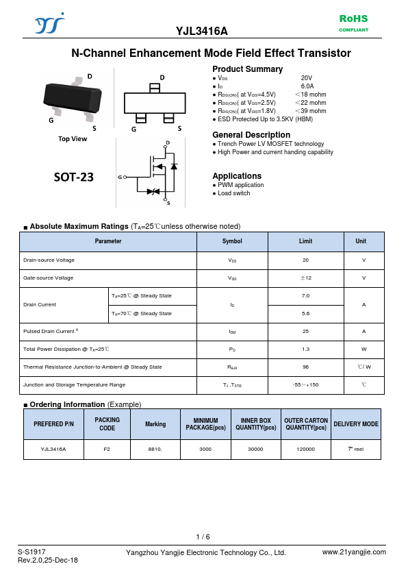
N-Channel Enhancement Mode Field Effect Transistor
Product Summary
- VDS
20V
- ID
- RDS(ON)( at VGS=4.5V)
- RDS(ON)( at VGS=2.5V)
- RDS(ON)( at VGS=1.8V)
6.0A <18 mohm <22 mohm <39 mohm
- ESD Protected Up to 3.5KV (HBM)
General Description
- Trench Power LV MOSFET technology
- High Power and current handing capability
Applications
- PWM application
- Load switch
-...