YJL02N10A Description
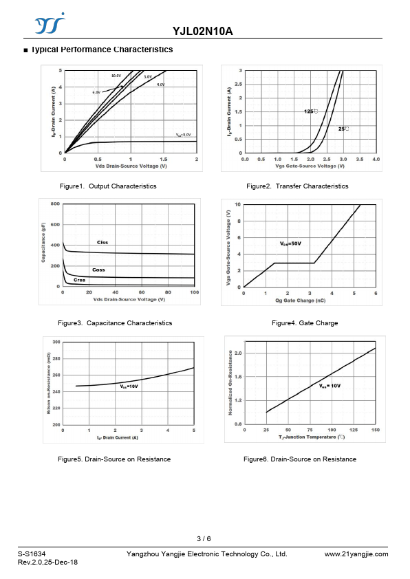
Pulse Width≤300us,Duty cycle ≤2%. Device mounted on FR-4 PCB, 1 inch x 0.85 inch x 0.062 inch. S-S1634 Rev.2.0,25-Dec-18 2/6 Yangzhou Yangjie Electronic Technology Co., Ltd.
YJL02N10A is N-Channel Enhancement Mode Field Effect Transistor manufactured by Yangjie Electronic.
| Part Number | Description |
|---|---|
| YJL03N06A | N-Channel Enhancement Mode Field Effect Transistor |
| YJL2300A | N-Channel Enhancement Mode Field Effect Transistor |
| YJL2301C | P-Channel Enhancement Mode Field Effect Transistor |
| YJL2302A | N-Channel Enhancement Mode Field Effect Transistor |
| YJL2305B | P-Channel Enhancement Mode Field Effect Transistor |
Pulse Width≤300us,Duty cycle ≤2%. Device mounted on FR-4 PCB, 1 inch x 0.85 inch x 0.062 inch. S-S1634 Rev.2.0,25-Dec-18 2/6 Yangzhou Yangjie Electronic Technology Co., Ltd.