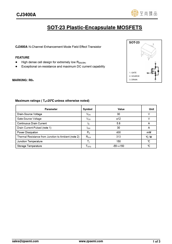
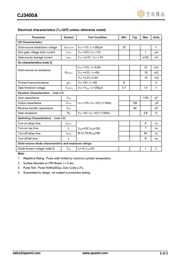
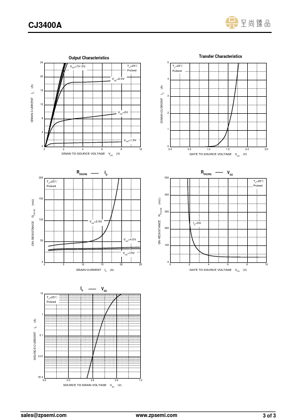
N-Channel Enhancement Mode Field Effect Transistor
Full PDF Text Transcription (Reference)
The following content is an automatically extracted verbatim text
from the original manufacturer datasheet and is provided for reference purposes only.
View original datasheet text
CJ3400A
SOT-23 Plastic-Encapsulate MOSFETS
CJ3400A N-Channel Enhancement Mode Field Effect Transistor
FEATURE z High dense cell design for extremely low RDS(ON) z Exceptional on-resistance and maximum DC current capability
MARKING: R0A
SOT-23
1. GATE 2. SOURCE 3. DRAIN
Maximum ratings ( Ta=25℃ unless otherwise noted)
Parameter
Drain-Source Voltage Gate-Source Voltage Continuous Drain Current Drain Current-Pulsed (note 1) Power Dissipation Thermal Resistance from Junction to Ambient (note 2) Junction Temperature Storage Temperature
Symbol
VDS VGS ID IDM PD RθJA TJ TSTG
Value
30 ±12 5.8 30 400 313 150 -55~+150
Unit
V V A A
mW ℃/W
℃ ℃
sales@zpsemi.com
www.zpsemi.