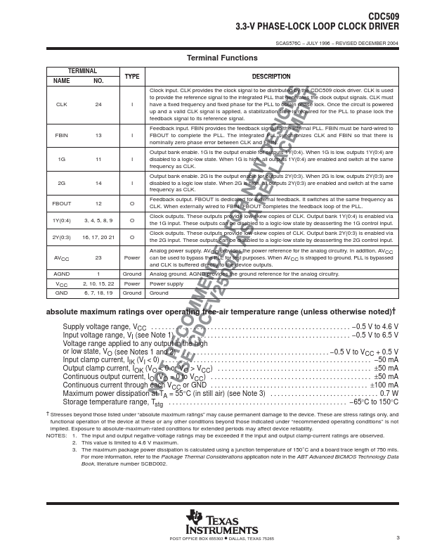
Datasheet Summary
CDC509 3.3ĆV PHASEĆLOCK LOOP CLOCK DRIVER
ą
SCAS576C
- JULY 1996
- REVISED DECEMBER 2004
D Use CDCVF2509A as a Replacement for this Device
D Phase-Lock Loop Clock Distribution for
Synchronous DRAM Applications
D Distributes One Clock Input to One Bank of
Five and One Bank of Four Outputs
D Separate Output Enable for Each Output
Bank
D External Feedback (FBIN) Pin Is Used to
Synchronize the Outputs to the Clock Input
D No External RC Network Required D Operates at 3.3-V VCC D Packaged in Plastic 24-Pin Thin Shrink
Small-Outline Package description
NOT REMENDED FOR NEW DESIGNS
PW PACKAGE (TOP VIEW)
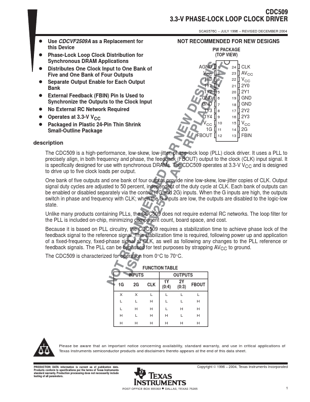
AGND 1 VCC 2 1Y0 3 1Y1 4 1Y2 5 GND 6 GND 7 1Y3 8 1Y4 9 VCC 10 1G 11
FBOUT 12
24 CLK 23...