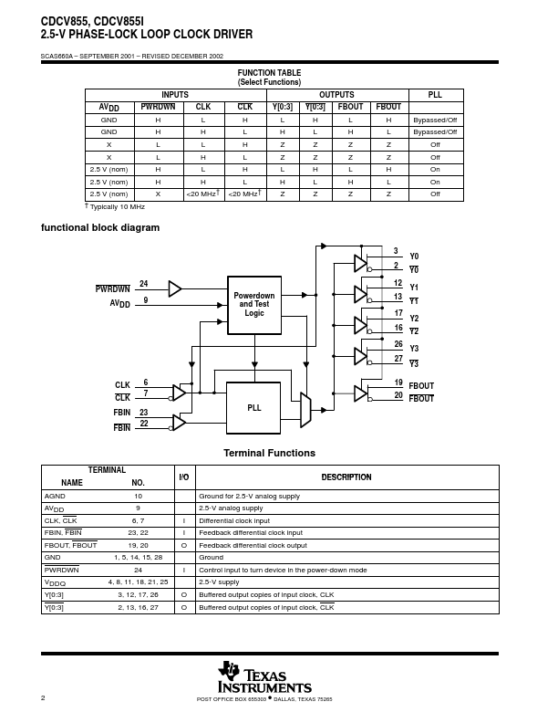
Datasheet Summary
CDCV855, CDCV855I 2.5-V PHASE-LOCK LOOP CLOCK DRIVER
D Phase-Lock Loop Clock Driver for Double
Data-Rate Synchronous DRAM Applications
D Spread Spectrum Clock patible D Operating Frequency: 60 MHz to 180 MHz D Low Jitter (cyc- cyc): ±50 ps D Distributes One Differential Clock Input to
Four Differential Clock Outputs
D Enters Low Power Mode and Three-State
Outputs When Input CLK Signal Is Less Than 20 MHz or PWRDWN Is Low
D Operates From Dual 2.5-V Supplies D 28-Pin TSSOP Package D Consumes < 200-µA Quiescent Current D External Feedback PIN (FBIN, FBIN) Are
Used to Synchronize the Outputs to the Input Clocks
SCAS660A
- SEPTEMBER 2001
- REVISED DECEMBER 2002
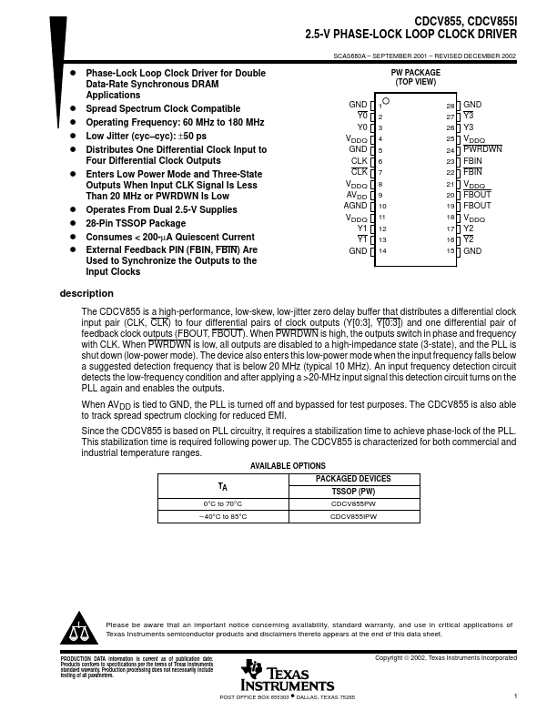
PW PACKAGE (TOP VIEW)
GND 1...