Datasheet Summary
Product Folder
Sample & Buy
Technical Documents
Tools & Software
Support & munity
SCAS666D
- JUNE 2001
- REVISED OCTOBER 2015
CDCVF2310 2.5-V to 3.3-V High-Performance Clock Buffer
1 Features
- 1 High-Performance 1:10 Clock Driver
- Operates up to 200 MHz at VDD 3.3 V
- Pin-to-Pin Skew < 100 ps at VDD 3.3 V
- VDD Range: 2.3 V to 3.6 V
- Operating Temperature Range
- 40°C to 105°C
- Supports 105ºC Ambient Temperature (see
Thermal Considerations)
- Output Enable Glitch Suppression
- Distributes One Clock Input to Two Banks of Five
Outputs
- 25-Ω On-Chip Series Damping Resistors
- Packaged in 24-Pin TSSOP
2 Applications
- General-Purpose Applications
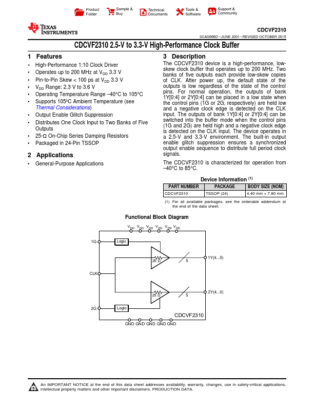
3 Description
The...