• Part: CDCVF2505
  • Description: 3.3-V Clock Phase-Lock Loop Clock Driver
  • Manufacturer: Texas Instruments
  • Size: 890.25 KB
Download CDCVF2505 Datasheet PDF
Texas Instruments
CDCVF2505
CDCVF2505 is 3.3-V Clock Phase-Lock Loop Clock Driver manufactured by Texas Instruments.
Features - 1 Phase-Lock Loop Clock Driver for Synchronous DRAM and General-Purpose Applications - Spread Spectrum Clock patible - Operating Frequency: 24 MHz to 200 MHz - Low Jitter (Cycle-to-Cycle): < |150 ps| (Over 66 MHz to 200 MHz Range) - Distributes One Clock Input to One Bank of Five Outputs (CLKOUT Used to Tune the Input-Output Delay) - Three-States Outputs When There Is No Input Clock - Operates From Single 3.3-V Supply - Available in 8-Pin TSSOP and 8-Pin SOIC Packages - Consumes Less Than 100 m A (Typical) in Power Down Mode - Internal Feedback Loop Is Used to Synchronize the Outputs to the Input Clock - 25-Ω On-Chip Series Damping Resistors - Integrated RC PLL Loop Filter Eliminates the Need for External ponents 2 Applications - Synchronous DRAMs - Industrial Applications - General-Purpose Zero-Delay Clock Buffers 3 Description 
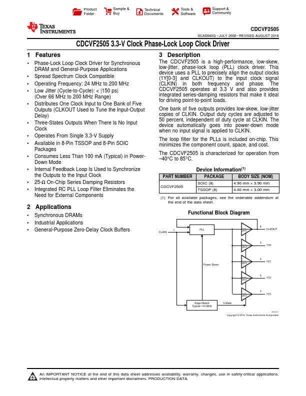
The CDCVF2505 is a high-performance, low-skew, low-jitter, phase-lock loop (PLL) clock driver. This device uses a PLL to precisely align the output clocks (1Y[0-3] and CLKOUT) to the input clock signal (CLKIN) in both frequency and phase. The CDCVF2505 operates at 3.3 V and also provides integrated series-damping resistors that make it ideal for driving point-to-point loads. One bank of five outputs provides low-skew, low-jitter copies of CLKIN. Output duty cycles are adjusted to 50 percent, independent of duty cycle at CLKIN. The device automatically goes into power-down mode when no input signal is applied to CLKIN. The loop filter for the PLLs is included on-chip. This minimizes the ponent count, space, and cost. The CDCVF2505 is characterized for operation from - 40°C to 85°C. Device Information(1) PART NUMBER PACKAGE BODY SIZE (NOM) SOIC (8) TSSOP (8) 4.90 mm × 3.90 mm 4.40 mm × 3.00 mm (1) For all available packages, see the orderable addendum at the end of the data sheet. Functional Block Diagram CLKIN 8 CLKOUT 25 W 3 1Y0 25 W Power...