CDCVF2509A Overview
Key Specifications
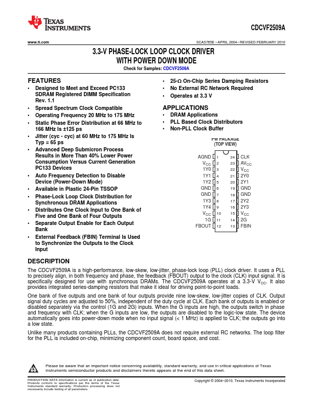
Package: TSSOP
Mount Type: Surface Mount
Pins: 24
Operating Voltage: 3.3 V
Description
The CDCVF2509A is a high-performance, low-skew, low-jitter, phase-lock loop (PLL) clock driver. It uses a PLL to precisely align, in both frequency and phase, the feedback (FBOUT) output to the clock (CLK) input signal.
Key Features
- Designed to Meet and Exceed PC133 SDRAM Registered DIMM Specification Rev. 1.1
- Spread Spectrum Clock Compatible
- Operating Frequency 20 MHz to 175 MHz
- Static Phase Error Distribution at 66 MHz to 166 MHz Is ±125 ps
- cyc) at 60 MHz to 175 MHz Is Typ = 65 ps