Datasheet4U Logo Datasheet4U.com

CDCVF2505-Q1 - 3.3-V CLOCK PHASE-LOCKED LOOP CLOCK DRIVER

General Description

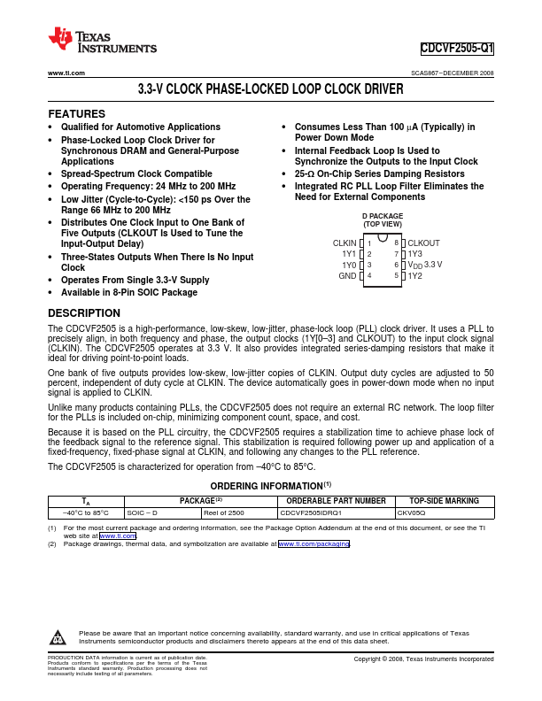
The CDCVF2505 is a high-performance, low-skew, low-jitter, phase-lock loop (PLL) clock driver.

3] and CLKOUT) to the input clock signal (CLKIN).

The CDCVF2505 operates at 3.3 V.

Key Features

  • 1.
  • Qualified for Automotive.

📥 Download Datasheet

Full PDF Text Transcription (Reference)

The following content is an automatically extracted verbatim text from the original manufacturer datasheet and is provided for reference purposes only.

View original datasheet text
CDCVF2505-Q1 www.ti.com........................................................................................................................................................................................... SCAS867 – DECEMBER 2008 3.3-V CLOCK PHASE-LOCKED LOOP CLOCK DRIVER FEATURES 1 • Qualified for Automotive Applications • Phase-Locked Loop Clock Driver for Synchronous DRAM and General-Purpose Applications • Spread-Spectrum Clock Compatible • Operating Frequency: 24 MHz to 200 MHz • Low Jitter (Cycle-to-Cycle): <150 ps Over the Range 66 MHz to 200 MHz • Distributes One Clock Input to One Bank of Five Outputs (CLKOUT Is Used to Tune the Input-Output Delay) • Three-States Outputs When There Is No Input Clock • Operates From Single 3.