Datasheet Summary
.ti.
SCAS771B
- AUGUST 2004
- REVISED JANUARY 2008
2.5-V TO 3.3-V HIGH-PERFORMANCE CLOCK BUFFER
Features
- High-Performance 1:10 Clock Driver
- Pin-to-Pin Skew < 100 ps at VDD 3.3 V
- VDD Range = 2.3 V to 3.6 V
- Input Clock Up To 200 MHz (See Figure 7)
- Operating Temperature Range
- 40°C to 85°C
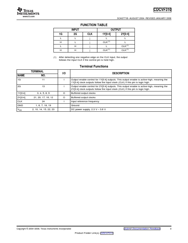
- Output Enable Glitch Suppression
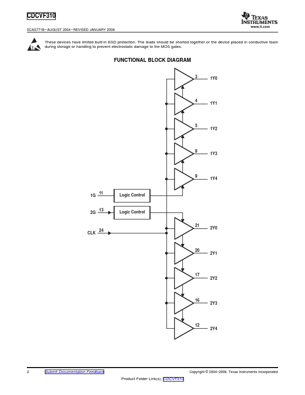
- Distributes One Clock Input to Two Banks of
Five Outputs
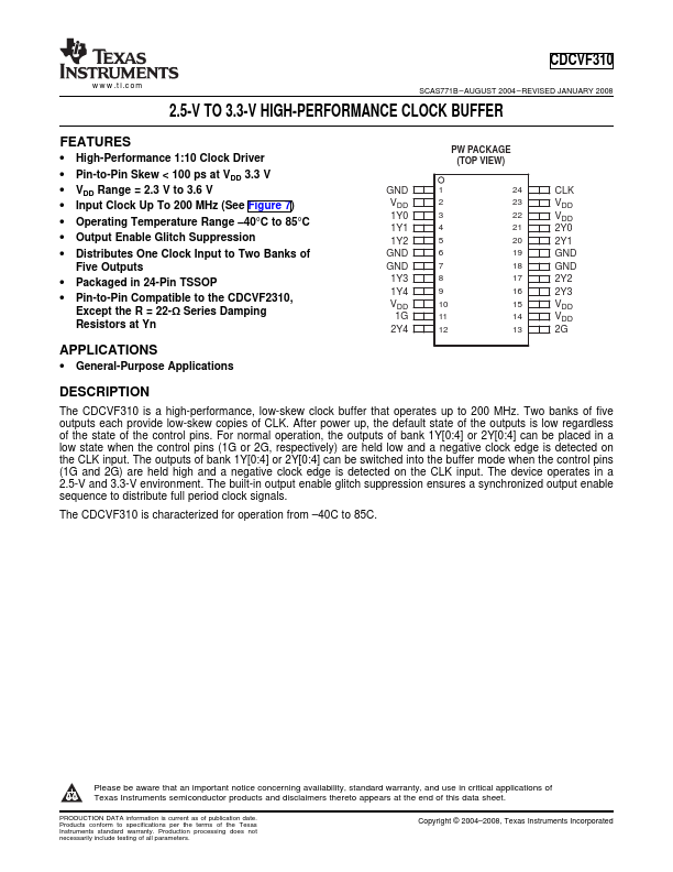
- Packaged in 24-Pin TSSOP
- Pin-to-Pin patible to the CDCVF2310,
Except the R = 22-Ω Series Damping Resistors at Yn
APPLICATIONS
- General-Purpose Applications
GND VDD 1Y0 1Y1 1Y2 GND GND 1Y3 1Y4 VDD
1G 2Y4
PW PACKAGE (TOP...