Datasheet4U Logo Datasheet4U.com

CSD18502KCS Datasheet Power MOSFETs

Manufacturer: Texas Instruments

General Description

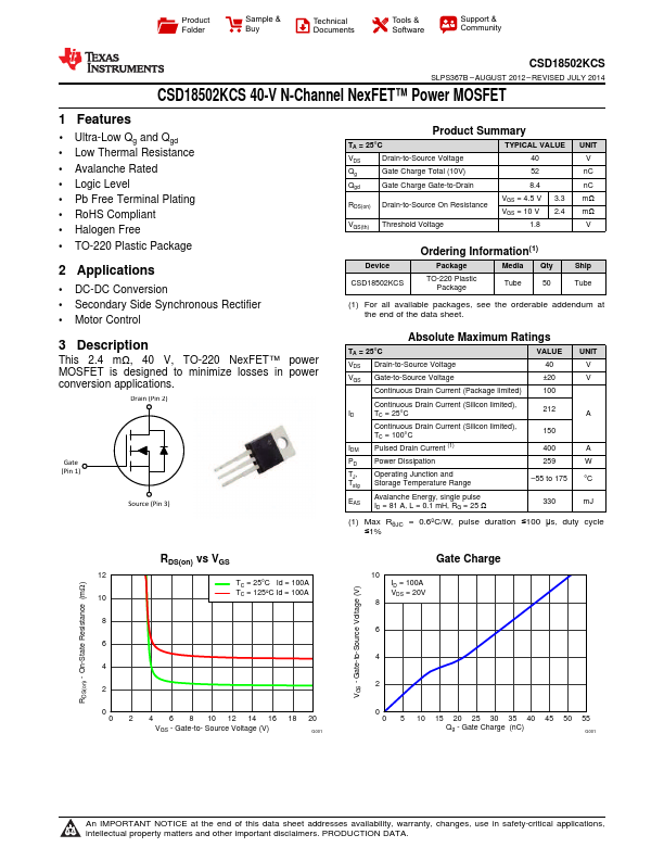
This 2.4 mΩ, 40 V, TO-220 NexFET™ power MOSFET is designed to minimize losses in power conversion applications.

Drain (Pin 2) Gate (Pin 1) Source (Pin 3) Product Summary TA = 25°C VDS Drain-to-Source Voltage Qg Gate Charge Total (10V) Qgd Gate Charge Gate-to-Drain RDS(on) Drain-to-Source On Resistance VGS(th) Threshold Voltage TYPICAL VALUE 40 52 8.4 VGS = 4.5 V 3.3 VGS = 10 V 2.4 1.8 UNIT V nC nC mΩ mΩ V Device CSD18502KCS Ordering Information(1) Package Media Qty TO-220 Plastic Package Tube 50 Ship Tube (1) For all available packages, see the orderable addendum at the end of the data sheet.

Absolute Maximum Ratings TA = 25°C VDS Drain-to-Source Voltage VGS Gate-to-Source Voltage Continuous Drain Current (Package limited) VALUE 40 ±20 100 UNIT V V Continuous Drain Current (Silicon limited), ID TC = 25°C 212 A Continuous Drain Current (Silicon limited), TC = 100°C 150 IDM Pulsed Drain Current (1) 400 A PD Power Dissipation 259 W TJ, Operating Junction and Tstg Storage Temperature Range –55 to 175 °C EAS Avalanche Energy, single pulse ID = 81 A, L = 0.1 mH, RG = 25 Ω 330 mJ (1) Max RθJC = 0.6ºC/W, pulse duration ≤100 μs, duty cycle ≤1% RDS(on) - On-State Resistance (mΩ) VGS - Gate-to-Source Voltage (V) RDS(on) vs VGS 12 TC = 25°C Id = 100A 10 TC = 125ºC Id = 100A 8 6 4 2 0 0 2 4 6 8 10 12 14 16 18 20 VGS - Gate-to- Source Voltage (V) G001 Gate Charge 10 ID = 100A VDS = 20V 8 6 4 2 0 0 5 10 15 20 25 30 35 40 45 50 55 Qg - Gate Charge (nC)

Overview

Product Folder Sample & Buy Technical Documents Tools & Software Support & Community CSD18502KCS SLPS367B – AUGUST 2012 – REVISED JULY 2014 CSD18502KCS 40-V N-Channel NexFET™ Power MOSFET.

Key Features

  • 1 Ultra-Low Qg and Qgd.
  • Low Thermal Resistance.
  • Avalanche Rated.
  • Logic Level.
  • Pb Free Terminal Plating.
  • RoHS Compliant.
  • Halogen Free.
  • TO-220 Plastic Package 2.