Datasheet4U Logo Datasheet4U.com

CSD18503KCS Datasheet 40V N-Channel Power MOSFET

Manufacturer: Texas Instruments

General Description

This 40V, 3.6mΩ, TO-220 NexFET™ power MOSFET has been designed to minimize losses in power conversion applications.

Drain (Pin 2) Gate (Pin 1) Source (Pin 3) 16 TC = 25°C Id = 75A 14 TC = 125ºC Id = 75A 12 10 8 6 4 2 0 0 2 4 6 8 10 12 14 16 18 20 VGS - Gate-to- Source Voltage (V) G001 RDS(on) vs VGS Product Summary TA = 25°C TYPICAL VALUE VDS Drain-to-Source Voltage 40 Qg Gate Charge Total (10V) 30 Qgd Gate Charge Gate-to-Drain 4.6 RDS(on) Drain-to-Source On-Resistance VGS = 4.5V VGS = 10V 5.4 3.6 VGS(th) Threshold Voltage 1.9 Device Ordering Information (1) Package Media Qty CSD18503KCS TO-220 Plastic Package Tube 50 UNIT V nC nC mΩ mΩ V Ship Tube (1) For all available packages, see the orderable addendum at the end of the data sheet.

Absolute Maximum Ratings TA = 25°C VDS Drain-to-Source Voltage VGS Gate-to-Source Voltage Continuous Drain Current (Package limited) VALUE 40 ±20 100 Continuous Drain Current (Silicon limited), ID TC = 25°C Continuous Drain Current (Silicon limited), TC = 100°C IDM Pulsed Drain Current (1) PD Power Dissipation TJ, Operating Junction and Tstg Storage Temperature Range EAS Avalanche Energy, single pulse ID = 57A, L = 0.1mH, RG = 25Ω 142 100 358 188 –55 to 175 162 UNIT V V A A W °C mJ (1) Max RθJC = 0.8°C/W, pulse duration ≤100μs, duty cycle ≤1% 10 ID = 75A VDS = 20V 8 6 4 2 0 0 5 10 15 20 25 30 Qg - Gate Charge (nC) G001 Gate Charge An IMPORTANT NOTICE at the end of this data sheet addresses availability, warranty, change

Overview

CSD18503KCS SLPS368B – SEPTEMBER 2012 – REVISED MARCH 2024 CSD18503KCS 40V N-Channel NexFET™ Power MOSFET
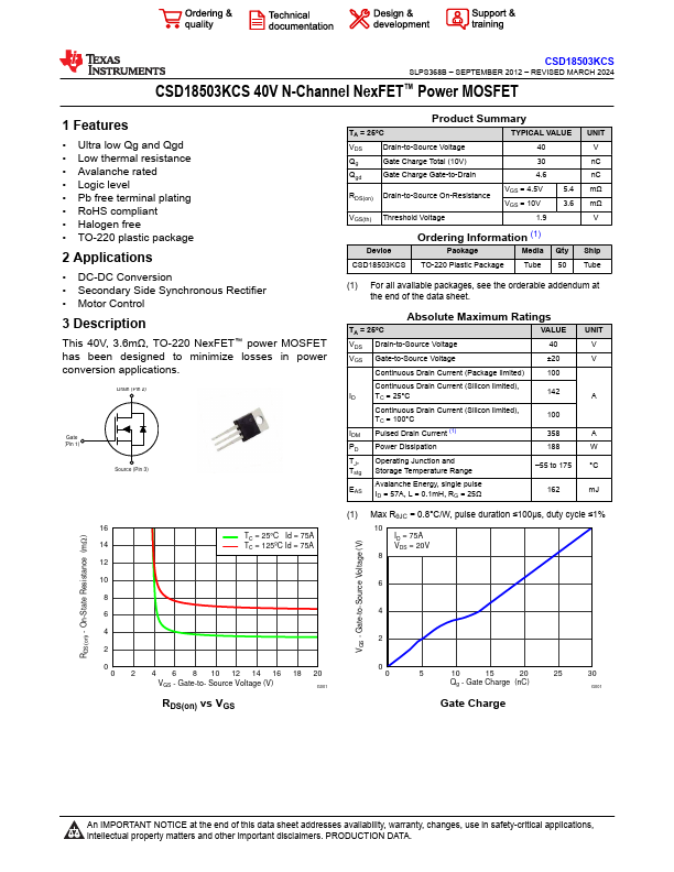
 RDS(on) - On-State Resistance (mΩ) VGS - Gate-to-Source Voltage (V).

Key Features

  • Ultra low Qg and Qgd.
  • Low thermal resistance.
  • Avalanche rated.
  • Logic level.
  • Pb free terminal plating.
  • RoHS compliant.
  • Halogen free.
  • TO-220 plastic package 2.