CSD23203W
Features
- 1 Ultra-Low Qg and Qgd
- Low RDS(on)
- Small Footprint
- Low Profile 0.62-mm Height
- Lead Free
- Ro HS pliant
- Halogen Free
- CSP 1-mm × 1.5-mm Wafer Level Package
2 Applications
- Battery Management
- Load Switch
- Battery Protection
3 Description
This 16.2-mΩ,
- 8-V, P-Channel device is designed to deliver the lowest on-resistance and gate charge in a small 1 × 1.5 mm outline with excellent thermal characteristics in an ultra-low profile.
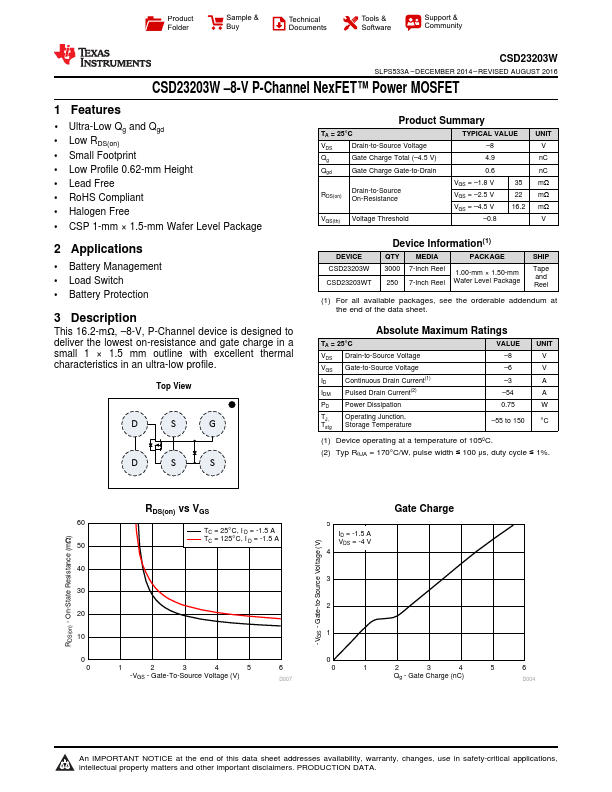
Top View
Product Summary
TA = 25°C
Drain-to-Source Voltage
Qg
Gate Charge Total (- 4.5 V)
Qgd
Gate Charge Gate-to-Drain
RDS(on)
Drain-to-Source On-Resistance
VGS(th) Voltage Threshold
TYPICAL VALUE
- 8
VGS =
- 1.8 V VGS...