Product
Folder
Sample &
Buy
Technical
Documents
Tools &
Software
Support &
Community
UCC27518A-Q1, UCC27519A-Q1
SLVSC90B – AUGUST 2013 – REVISED AUGUST 2015
UCC2751xA-Q1 Single-Channel High-Speed Low-Side Gate Driver With Negative Input
Voltage Capability
1 Features
•1 Qualified for Automotive Applications
• AEC-Q100 Qualified With the Following Results:
– Device Automotive Qualified Grade 1: –40°C
to +125°C Ambient Operating Temperature
Range
– Device HBM ESD Classification Level 2
– Device CDM ESD Classification Level C6
• Low-Cost Gate-Driver Device Offering Superior
Replacement of NPN and PNP Discrete Solutions
• Pin-to-Pin Compatible With TI's TPSS2828-Q1
and the TPS2829-Q1
• 4-A Peak Source and 4-A Peak Sink Symmetrical
Drive
• Fast Propagation Delays (17-ns typical)
• Fast Rise and Fall Times (8-ns and 7-ns typical)
• 4.5-V to 18-V Single Supply Range
• Outputs Held Low During VDD UVLO (Ensures
Glitch-Free Operation at Power-Up and Power-
Down)
• CMOS Input Logic Threshold (Function of Supply
Voltage With Hysteresis)
• Hysteretic Logic Thresholds for High Noise
Immunity
• EN Pin for Enable Function (Allowed to be no
Connect)
• Ability to Support Negative Voltages (–5 V) at
Input and Enable pins
• Output Held Low when Input Pins are Floating
• Input Pin Absolute Maximum Voltage Levels Not
Restricted by VDD Pin Bias Supply Voltage
• Operating Temperature Range of –40°C to 140°C
• 5-Pin DBV Package (SOT-23)
2 Applications
• Automotive
• Switch-Mode Power Supplies
• DC-to-DC Converters
• Companion Gate Driver Devices for Digital Power
Controllers
• Solar Power, Motor Control, UPS
• Gate Driver for Emerging Wide Band-Gap Power
Devices (such as GaN)
3 Description
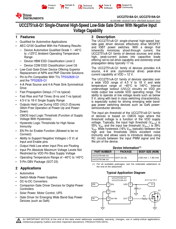
The UCC2751xA-Q1 single-channel high-speed low-
side gate driver devices effectively drive MOSFET
and IGBT power switches. With a design that
inherently minimizes shoot-through current, the
UCC2751xA-Q1 family of devices sources and sinks
high, peak-current pulses into capacitive loads
offering rail-to-rail drive capability and extremely small
propagation delay typically 17 ns.
The UCC2751xA-Q1 family of devices provides 4-A
source, 4-A sink (symmetrical drive) peak-drive
current capability at VDD = 12 V.
The UCC2751xA-Q1 family of devices operates over
a wide VDD range of 4.5 V to 18 V and wide
temperature range of –40°C to 140°C. Internal
undervoltage lockout (UVLO) circuitry on VDD pin
holds output low outside VDD operating range. The
ability to operate at low voltage levels such as below
5 V, along with best in class switching characteristics,
is especially suited for driving emerging wide band-
gap power switching devices such as GaN power-
semiconductor devices.
The input pin threshold of the UCC2751xA-Q1 family
of devices is based on CMOS logic where the
threshold voltage is a function of the VDD supply
voltage. Typically, the input high threshold (VIN–H) is
55% VDD and the input low threshold (VIN–L) is 39%
VDD. Wide hysteresis (16% VDD typically) between the
high and low thresholds offers excellent noise
immunity and allows users to introduce delays using
RC circuits between the input PWM signal and the
INx pin of the device.
Device Information(1)
PART NUMBER
PACKAGE
BODY SIZE (NOM)
UCC27518A-Q1
UCC27519A-Q1
SOT-23 (5)
2.90 mm × 1.60 mm
(1) For all available packages, see the orderable addendum at
the end of the datasheet.
Typical Application Diagram
UCC27518A-Q1
UCC27519A-Q1
EN
1 EN
VDD 5
4.5 V to 18 V
V+
2 GND
C1
Q1
R1
IN
3 IN+/IN-
OUT 4
1
An IMPORTANT NOTICE at the end of this data sheet addresses availability, warranty, changes, use in safety-critical applications,
intellectual property matters and other important disclaimers. PRODUCTION DATA.