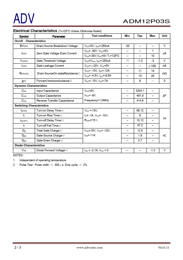
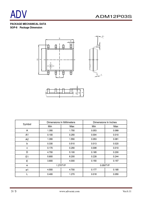
Click to expand full text
ADV
ADM12P03S
P-Channel Logic Level Enhancement Mode Field Effect Transistor
PRODUCT SUMMARY
VDSS -30V
ID -12A
RDS(ON) (mΩ) 14mΩ
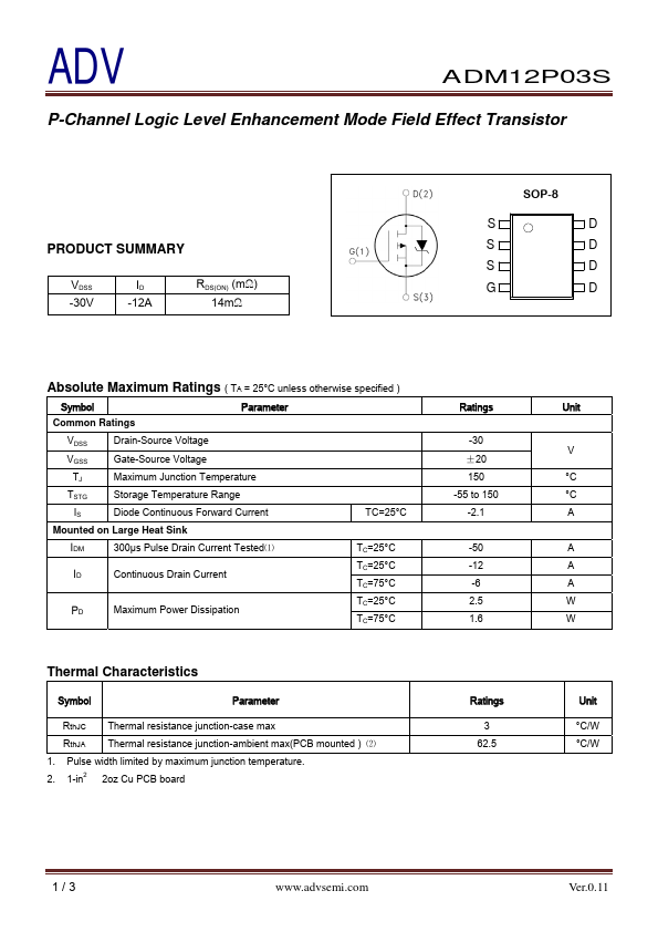
SOP-8
S
D
S
D
S
D
G
D
Absolute Maximum Ratings ( TA = 25°C unless otherwise specified )
Symbol
Parameter
Common Ratings
VDSS
Drain-Source Voltage
VGSS
Gate-Source Voltage
TJ
Maximum Junction Temperature
TSTG
Storage Temperature Range
IS
Diode Continuous Forward Current
TC=25°C
Mounted on Large Heat Sink
IDM
300μs Pulse Drain Current Tested⑴
ID
Continuous Drain Current
PD
Maximum Power Dissipation
TC=25°C TC=25°C TC=75°C TC=25°C TC=75°C
Thermal Characteristics
Symbol
Parameter
RthJC Thermal resistance junction-case max RthJA Thermal resistance junction-ambient max(PCB mounted ) ⑵ 1.
 ADM12P03S Datasheet