Datasheet Details
| Part number | AS4C512M16D3LA |
|---|---|
| Manufacturer | Alliance Semiconductor |
| File Size | 1.92 MB |
| Description | 8Gbit DDR3L SDRAM |
| Datasheet |
 AS4C512M16D3LA-AllianceSemiconductor.pdf AS4C512M16D3LA-AllianceSemiconductor.pdf
|
| Part number | AS4C512M16D3LA |
|---|---|
| Manufacturer | Alliance Semiconductor |
| File Size | 1.92 MB |
| Description | 8Gbit DDR3L SDRAM |
| Datasheet |
AS4C512M16D3LA-AllianceSemiconductor.pdf
|
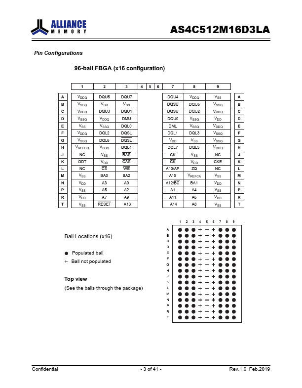
Pin CK, CK CKE CS ODT RAS, CAS, WE DM BA0 - BA2 A0 - A15 A10 / AP A12 / BC RESET DQ DQSL, DQSL DQSU, DQSU NC Type Input Input Input Input Input Input Input Input Input Input Input Input/ Output Input/ Output Function Clock : CK and CK are differential clock inputs.All address and control input signals are sampled on the crossing of the positive edge of CK and negative edge of CK.Output (read) data is referenced to the crossings of CK and CK Clock Enable : CKE HIGH activates, and CKE Low dea
📁 AS4C512M16D3LA Similar Datasheet