Datasheet Details
- Part number
- ADG884
- Manufacturer
- Analog Devices ↗
- File Size
- 297.59 KB
- Datasheet
- ADG884_AnalogDevices.pdf
- Description
- DUAL 2:1 MUX/SPDT AUDIO SWITCH
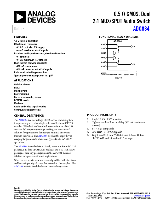
The ADG884 is a low voltage CMOS device containing two independently selectable single-pole, double-throw (SPDT) switches..
📁 Related Datasheet
📌 All Tags
ADG884 Stock/Price