Datasheet Details
| Part number | CY2509 |
|---|---|
| Manufacturer | Cypress Semiconductor |
| File Size | 276.00 KB |
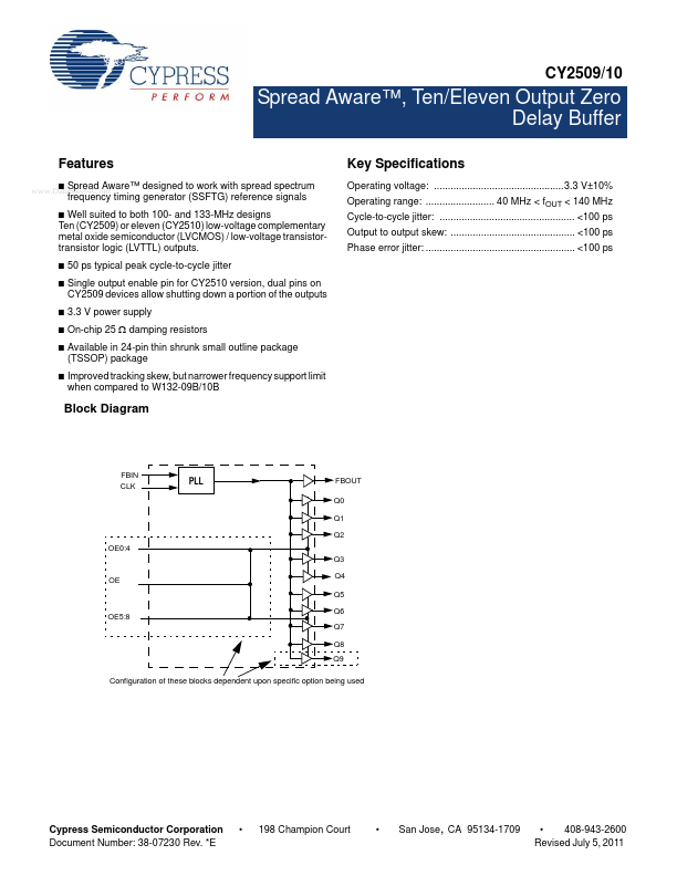
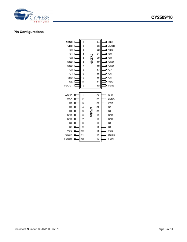
| Description | (CY2509 / CY2510) Ten/Eleven Output Zero Delay Buffer |
| Datasheet |
 CY2509 Datasheet CY2509 Datasheet
|
| Note |
This datasheet PDF includes multiple part numbers: CY2509, CY2510. Please refer to the document for exact specifications by model. |
|
|