Datasheet Details
| Part number | CY2510 |
|---|---|
| Manufacturer | Cypress Semiconductor |
| File Size | 276.00 KB |
| Description | (CY2509 / CY2510) Ten/Eleven Output Zero Delay Buffer |
| Datasheet |
 CY2510 Datasheet CY2510 Datasheet
|
|
|
| Part number | CY2510 |
|---|---|
| Manufacturer | Cypress Semiconductor |
| File Size | 276.00 KB |
| Description | (CY2509 / CY2510) Ten/Eleven Output Zero Delay Buffer |
| Datasheet |
CY2510 Datasheet
|
|
|
|
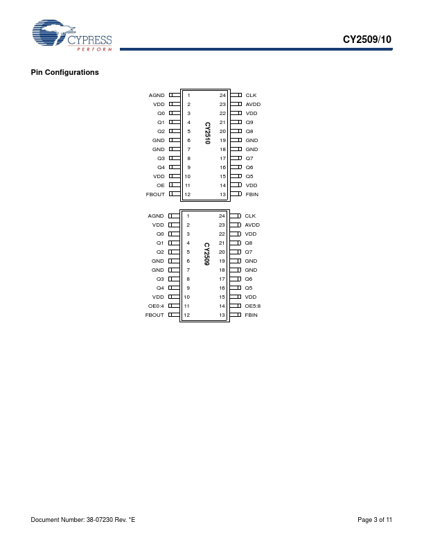
Reference input: Output signals Q0:9 will be synchronized to this signal.
📁 Similar Datasheet