Datasheet Details
| Part number | CY28343 |
|---|---|
| Manufacturer | Cypress Semiconductor |
| File Size | 91.83 KB |
| Description | Zero Delay SDR/DDR Clock Buffer |
| Datasheet |
 CY28343 Datasheet CY28343 Datasheet
|
|
|
| Part number | CY28343 |
|---|---|
| Manufacturer | Cypress Semiconductor |
| File Size | 91.83 KB |
| Description | Zero Delay SDR/DDR Clock Buffer |
| Datasheet |
CY28343 Datasheet
|
|
|
|
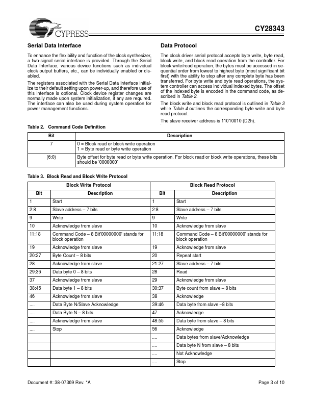
2, 3] Pin 10 47 23 30,32,36,38 42,44 29,31,35,37 41,43 2-5,8,9 15-18,21 46 Name CLKIN FBIN_DDR FBIN_SDR DDRT(0:5) DDRC(0:5) SDRAM(0:12) FBOUT_DDR I/O I I PD I PD O O O O Clock Input.Reference the PLL Feedback Clock Output.Connect to FBOUT_DDR for accessing the PLL.See Function Table on page 1 Feedback Clock Input.Connect to FBOUT_SDR for accessing the PLL.See Function Table on page 1 Clock Outputs.True copies of the CLKIN input Clock Outputs.Complementary copies of the CLKIN input Clock O
📁 Similar Datasheet