Datasheet Details
| Part number | CY28347 |
|---|---|
| Manufacturer | Cypress Semiconductor |
| File Size | 237.28 KB |
| Description | Universal Single-chip Clock Solution |
| Datasheet |
 CY28347 Datasheet CY28347 Datasheet
|
|
|
| Part number | CY28347 |
|---|---|
| Manufacturer | Cypress Semiconductor |
| File Size | 237.28 KB |
| Description | Universal Single-chip Clock Solution |
| Datasheet |
CY28347 Datasheet
|
|
|
|
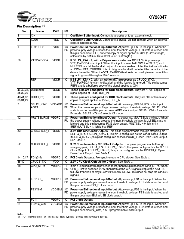
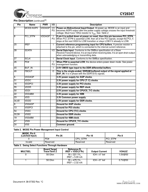
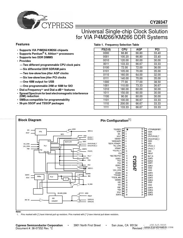
Pin 3 4 1 XIN XOUT FS0/REF0 VDD VDD [2] Name PWR I/O I O Description Oscillator Buffer Input.Connect to a crystal or to an external clock.Oscillator Buffer Output.Connect to a crystal.Do not connect when an external clock is applied at XIN.I/O Power-on Bidirectional Input/Output.At power-up, FS0 is the input.When the PU power supply voltage crosses the input threshold voltage, FS0 state is latched and this pin becomes REF0, buffered copy of signal applied at XIN.(1 2 x stren
📁 Similar Datasheet