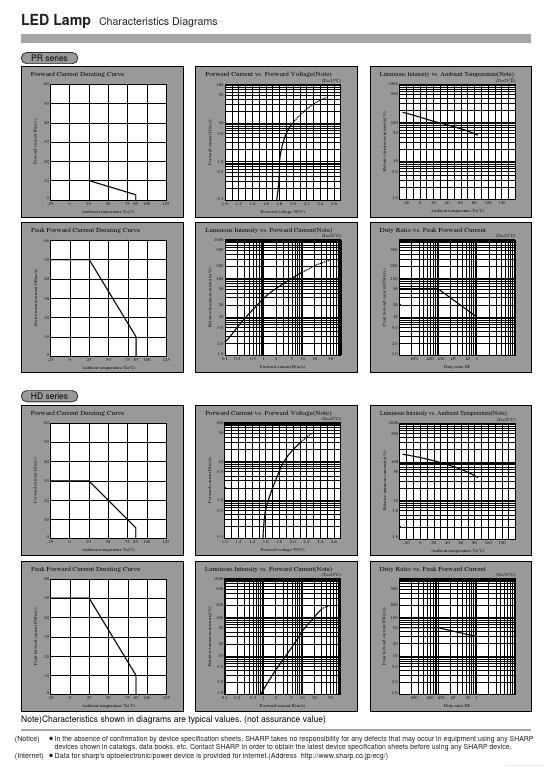
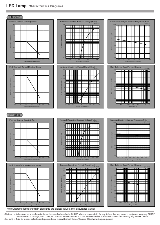
Click to expand full text
Leadless Chip LED Device
LT1t40A series
LT1t40A series
s Outline Dimensions
(Unit : mm)
2125 Size, 0.8mm Thickness, Leadless Chip LED Devices
s Radiation Diagram
(Ta=25˚C)
-20˚
Relative luminous intensity(%) 2.0 0.8
0˚ 100 80 60 40 20 0
X
+20˚ +40˚
-40˚
1.25
1
2 Cathode mark Recommended PWB pattern for soldering Device center 1.2 1.1
-60˚
+60˚
-80˚
+80˚
0.5
0.3
1.25
1.1
1.25
-20˚ -40˚
Relative luminous intensity(%) 1.Plating area Resist 2.Pin connections 1 Cathode 2 Anode 1 3.Unspecified tolerance:±0.1
0˚ 100 80 60 40 20 0
Y
+20˚ +40˚
0.4
0.4
2
-60˚
+60˚
-80˚
+80˚
U type: There is Anode mark on the device because polarity faces in the opposite direction.
s Absolute Maximum Ratings
Model No.
 LT1E40A Datasheet