Description
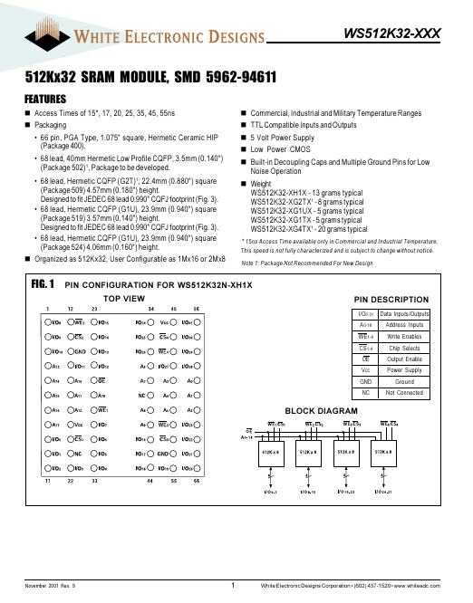
I/O0-31 A 0-18 WE 1-4 CS 1-4 OE VCC GND NC Data Inputs/Outputs Address Inputs Write Enables Chip Selects Output Enable Power Supply Ground Not Connected
BLOCK DIAGRAM
November 2001 Rev.9
1
White Electronic Designs Corporation (602) 437-1520 www.whiteedc.com
WS512K32-XXX
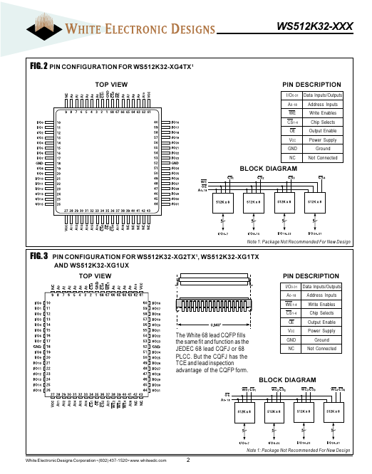
FIG.2 PIN CONFIGURATION FOR WS512K32-XG4TX1
TOP VIEW PIN DESCRIPTION
I/O0-31 A 0-18 WE CS 1-4 OE VCC GND NC Data Inputs/Outputs Address Inputs Write Enables Chip Selects Output Enable Power Supply Ground Not Connected
Features
- n Access Times of 15.
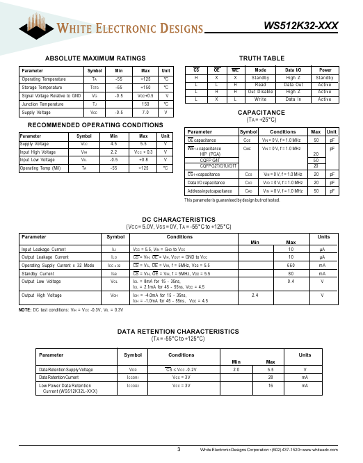
- , 17, 20, 25, 35, 45, 55ns n Packaging 66 pin, PGA Type, 1.075" square, Hermetic Ceramic HIP (Package 400). 68 lead, 40mm Hermetic Low Profile CQFP, 3.5mm (0.140") (Package 502)1, Package to be developed. 68 lead, Hermetic CQFP (G2T)1, 22.4mm (0.880") square (Package 509) 4.57mm (0.180") height. Designed to fit JEDEC 68 lead 0.990" CQFJ footprint (Fig. 3). 68 lead, Hermetic CQFP (G1U), 23.9mm (0.940") square (Package 519) 3.57mm (0.140") height. Designed to fit J.
 WS512K32_ETC.pdf