Description
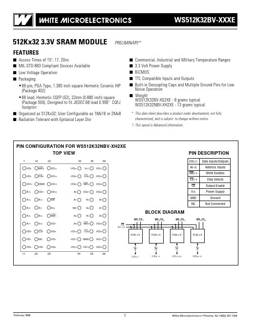
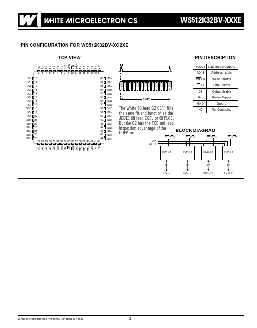
I/O0-31 A0-18 WE1-4 CS1-4
I/O29 I/O28 A0 A1
Data Inputs/Outputs Address Inputs Write Enables Chip Selects Output Enable Power Supply Ground Not Connected
OE VCC GND NC
BLOCK DIAGRAM
A2
WE1 CS 1 WE2 CS2 WE3 CS 3 WE 4CS4
I/O23 I/O22
OE A0-18 512K x 8 512K x 8
512K x 8
512K x 8
I/O21 I/O20 66
I/O0-7 I/O8-15 I/O16-23 I/O24-31
8 8 8 8
February 1998
1
White Microelectronics
Phoenix, AZ
(602) 437-1520
WS512K32BV-XXXE
PIN CONFIGURATION FOR WS512K32BV-XG2XE TOP VIEW
NC A0
Features
- s Access Times of 15†, 17, 20ns s MIL-STD-883 Compliant Devices Available s Low Voltage Operation s Packaging.
- 66-pin, PGA Type, 1.385 inch square Hermetic Ceramic HIP (Package 402).
- 68 lead, Hermetic CQFP (G2), 22mm (0.880 inch) square (Package 500). Designed to fit JEDEC 68 lead 0.990" CQFJ footprint s Organized as 512Kx32; User Configurable as 1Mx16 or 2Mx8 s Radiation Tolerant with Epitaxial Layer Die s s s s s Commercial, Industrial and Military Temperature Ranges 3.3 Volt.
 WS512K32BV_ETC.pdf