Datasheet4U Logo Datasheet4U.com

XRK39653 8-OUTPUT ZERO DELAY BUFFER

📥 Download Datasheet  Datasheet Preview Page 1

Description

www.DataSheet4U.com xr FEBRUARY 2006 PRELIMINARY XRK39653 REV.P1.0.0 3.3V, 8-OUTPUT ZERO DELAY BUFFER use.The second is a full bypass mode that .
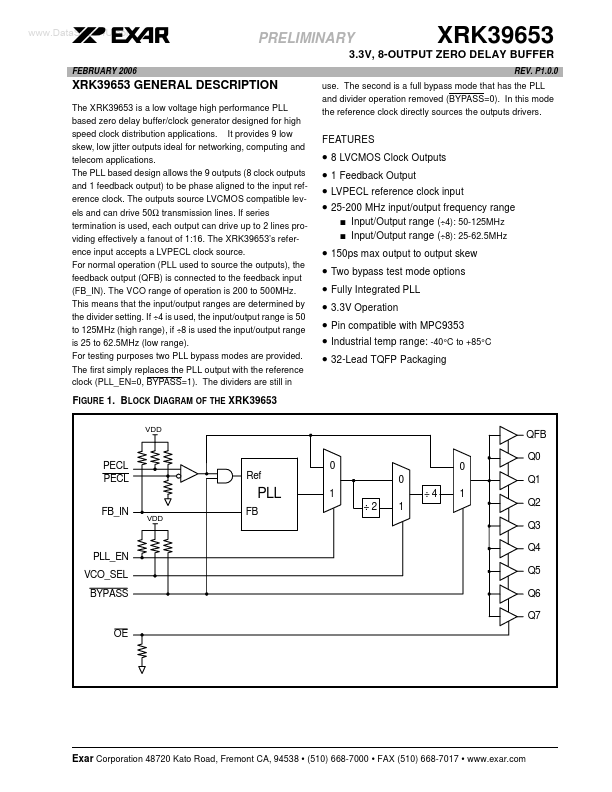
The XRK39653 is a low voltage high performance PLL based zero delay buffer/clock generator designed for high speed clock distribution applications.

📥 Download Datasheet

Preview of XRK39653 PDF
datasheet Preview Page 2 datasheet Preview Page 3

Datasheet Specifications

Part number
XRK39653
Manufacturer
Exar Corporation
File Size
123.89 KB
Datasheet
XRK39653_ExarCorporation.pdf
Description
8-OUTPUT ZERO DELAY BUFFER

Features

* 8 LVCMOS Clock Outputs 1 Feedback Output LVPECL reference clock input 25-200 MHz input/output frequency range
* Input/Output range (÷4): 50-125MHz
* Input/Output range (÷8): 25-62.5MHz
* 150ps max output to output skew
* Two bypass t

Applications

* It provides 9 low skew, low jitter outputs ideal for networking, computing and telecom applications. The PLL based design allows the 9 outputs (8 clock outputs and 1 feedback output) to be phase aligned to the input reference clock. The outputs source LVCMOS compatible levels and can drive 50Ω tran

XRK39653 Distributors

📁 Related Datasheet

📌 All Tags

Exar Corporation XRK39653-like datasheet