Datasheet Details
| Part number | XRK32309 |
|---|---|
| Manufacturer | Exar Corporation |
| File Size | 189.58 KB |
| Description | LOW-COST 3.3V ZERO DELAY BUFFER |
| Datasheet |
 XRK32309 Datasheet XRK32309 Datasheet
|
|
|
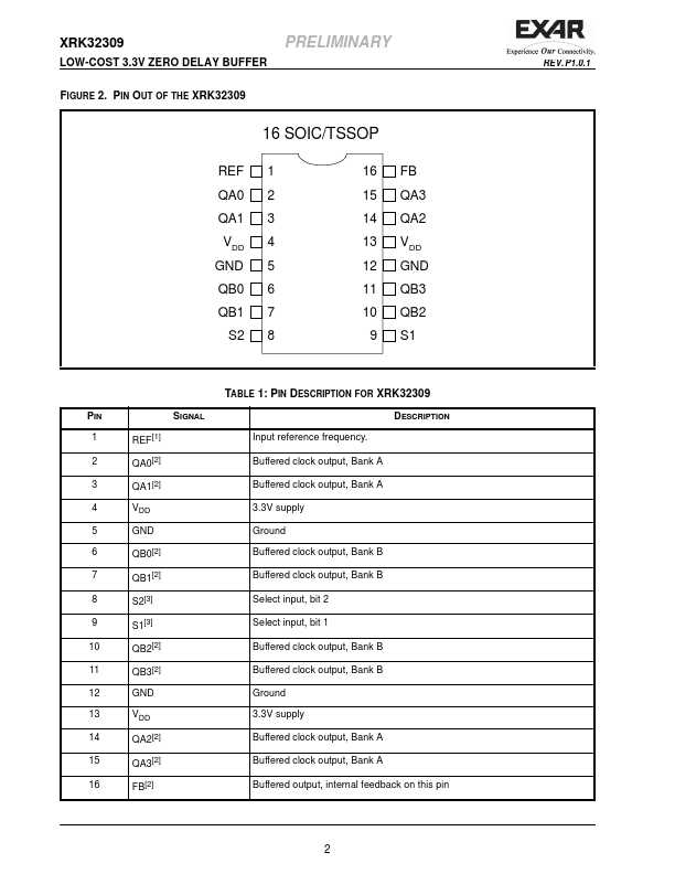
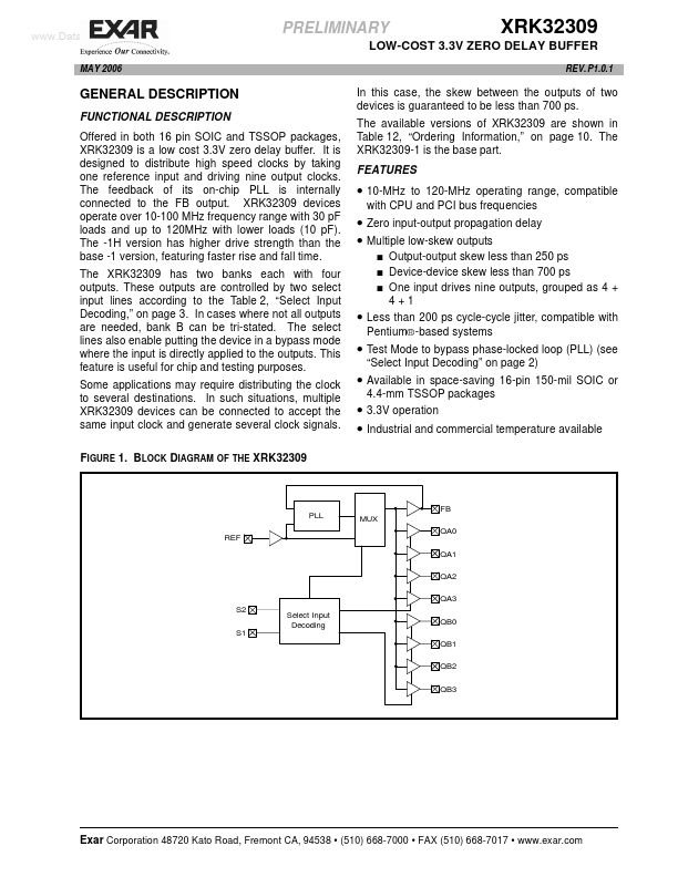
FUNCTIONAL DESCRIPTION Offered in both 16 pin SOIC and TSSOP packages, XRK32309 is a low cost 3.3V zero delay buffer.
It is designed to distribute high speed clocks by taking one reference input and driving nine output clocks.
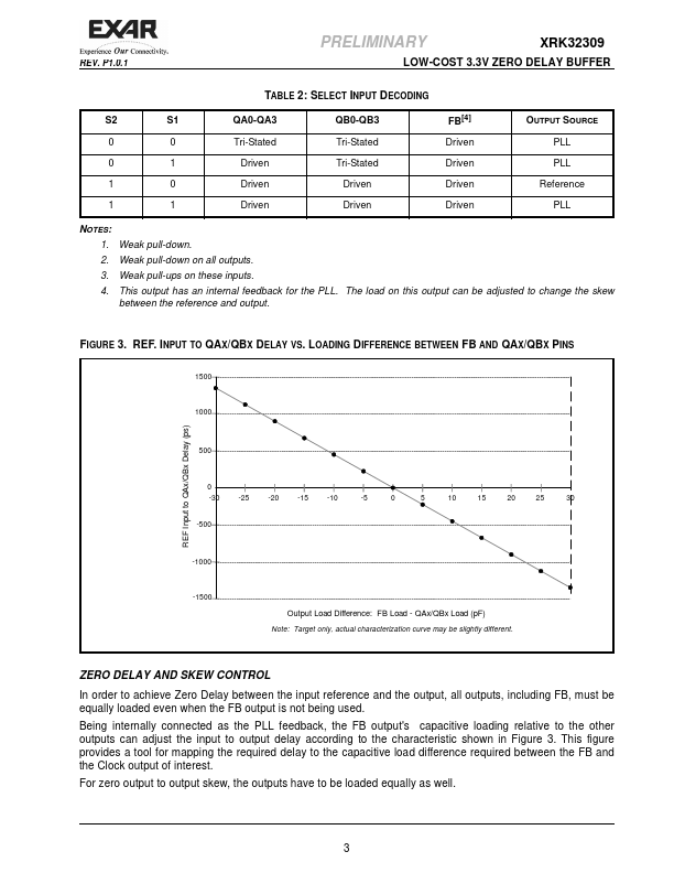
The feedback of its on-chip PLL is internally connected to the FB output.
| Part number | XRK32309 |
|---|---|
| Manufacturer | Exar Corporation |
| File Size | 189.58 KB |
| Description | LOW-COST 3.3V ZERO DELAY BUFFER |
| Datasheet |
XRK32309 Datasheet
|
|
|
|