XRK39653
XRK39653 is 8-OUTPUT ZERO DELAY BUFFER manufactured by Exar.
DESCRIPTION
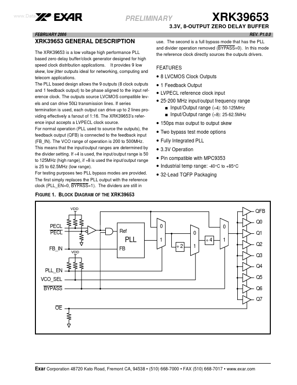
The XRK39653 is a low voltage high performance PLL based zero delay buffer/clock generator designed for high speed clock distribution applications. It provides 9 low skew, low jitter outputs ideal for networking, puting and tele applications. The PLL based design allows the 9 outputs (8 clock outputs and 1 feedback output) to be phase aligned to the input reference clock. The outputs source LVCMOS patible levels and can drive 50Ω transmission lines. If series termination is used, each output can drive up to 2 lines providing effectively a fanout of 1:16. The XRK39653’s reference input accepts a LVPECL clock source. For normal operation (PLL used to source the outputs), the feedback output (QFB) is connected to the feedback input (FB_IN). The VCO range of operation is 200 to 500MHz. This means that the input/output ranges are determined by the divider setting. If ÷4 is used, the input/output range is 50 to 125MHz (high range), if ÷8 is used the input/output range is 25 to 62.5MHz (low range). For testing purposes two PLL bypass modes are provided. The first simply replaces the PLL output with the reference clock (PLL_EN=0, BYPASS=1). The dividers are still in
FEATURES
- -
- -
8 LVCMOS Clock Outputs 1 Feedback Output LVPECL reference clock input 25-200 MHz input/output frequency range
- Input/Output range (÷4): 50-125MHz
- Input/Output range (÷8): 25-62.5MHz
- 150ps max output to output skew
- Two bypass test mode options
- -
- -
- Fully Integrated PLL 3.3V Operation Pin patible with MPC9353 Industrial temp range: -40°C to +85°C 32-Lead TQFP Packaging
FIGURE 1. BLOCK DIAGRAM OF THE XRK39653
QFB 0 0 1 ÷2 1 ÷4 1 Q0 0 Q1 Q2 Q3 Q4 Q5 Q6 Q7
PECL PECL FB_IN
Ref
PLL_EN VCO_SEL BYPASS
Exar Corporation 48720 Kato Road, Fremont CA, 94538
- (510) 668-7000
- FAX (510) 668-7017
- .exar.
XRK39653 3.3V, 8-OUTPUT ZERO DELAY BUFFER
PRELIMINARY
PRODUCT ORDERING INFORMATION
PRODUCT NUMBER XRK39653IQ XRK39653IQ-F PACKAGE TYPE 32-Lead TQFP...