XRK32510
XRK32510 is 3.3V PHASE-LOCK LOOP CLOCK DRIVER manufactured by Exar.
DESCRIPTION
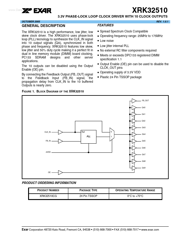
The XRK32510 is a high performance, low jitter, low skew clock driver. The XRK32510 uses phase-lock loop (PLL) tecnology to synthesize the CLK_IN signal into 10 output signals (QA), synchronized in both phase and frequency. XRK32510 features low skew, low jitter and 50% duty cycle making it a perfect fit in dual in line memory module (DIMM) board clocking, PC133 SDRAM designs and other server applications. The 10 outputs can be disabled using the Output Enable (OE) pin. By connecting the Feedback Output (FB_OUT) signal to the Feedback Input (FB_IN) signal, the propagation delay from CLK_IN to the 10 buffered Outputs is nearly zero. FIGURE 1. BLOCK DIAGRAM OF THE XRK32510
FEATURES
- Spread Spectrum Clock patible
- Operating frequency range: 25MHz to 175MHz
- Low noise
- Low jitter internal PLL
- No external RC filter ponents required
- Meets or exceeds DPC133 registered DIMM specification 1.1
- Output Enable (OE) pin can be used to disable the
CLCK_OUT pins
- Operating supply of 3.3V VDD
- Plastic 24 Pin TSSOP package
FB_OUT
QA0
QA1
QA2
QA3 CLK_IN
Ref
QA4
FB_IN
QA5
QA6 AVDD QA7
QA8
QA9 OE
PRODUCT ORDERING INFORMATION
PRODUCT NUMBER XRK32510CG PACKAGE TYPE 24 Pin TSSOP OPERATING TEMPERATURE RANGE 0°C to +70°C
Exar Corporation 48720 Kato Road, Fremont CA, 94538
- (510) 668-7000
- FAX (510) 668-7017
- .exar.
XRK32510 3.3V PHASE-LOCK LOOP CLOCK DRIVER WITH 10 CLOCK OUTPUTS FIGURE 2. PIN OUT OF THE XRK32510 xr
REV. 1.0.1
AGND VDD QA0 QA1 QA2 GND GND QA3 QA4 VDD OE FB_OUT
1 2 3 4 5 6 7 8 9 10 11 12
24 23 22 21 20 19 18 17 16 15 14 13
CLK_IN AVDD VDD QA9 QA8 GND GND QA7 QA6 QA5 VDD...