Datasheet Details
| Part number | XRK32308 |
|---|---|
| Manufacturer | Exar Corporation |
| File Size | 193.27 KB |
| Description | 3.3V ZERO DELAY BUFFER |
| Datasheet |
 XRK32308 Datasheet XRK32308 Datasheet
|
|
|
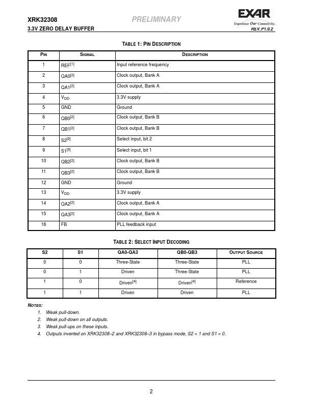
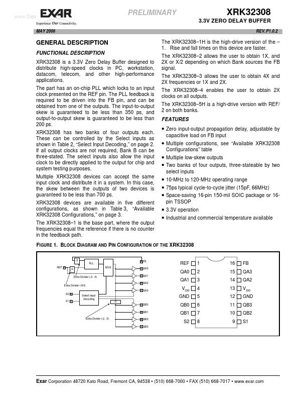
FUNCTIONAL DESCRIPTION XRK32308 is a 3.3V Zero Delay Buffer designed to distribute high-speed clocks in PC, workstation, datacom, telecom, and other high-performance applications.
The part has an on-chip PLL which locks to an input clock presented on the REF pin.
| Part number | XRK32308 |
|---|---|
| Manufacturer | Exar Corporation |
| File Size | 193.27 KB |
| Description | 3.3V ZERO DELAY BUFFER |
| Datasheet |
XRK32308 Datasheet
|
|
|
|