BC517
Overview
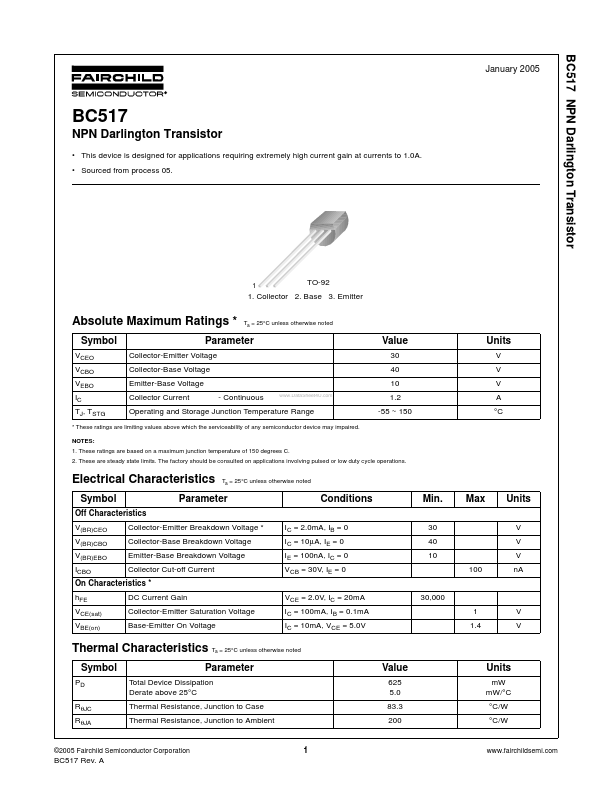
BC517 NPN Darlington Transistor January 2005 BC517 NPN Darlington Transistor • This device is designed for applications requiring extremely high current gain at currents to 1.0A. • Sourced from proc...
| Part | BC517 |
|---|---|
| Description | NPN Darlington Transistor |
| Category | Transistor |
| Manufacturer | Fairchild Semiconductor |
| Size | 54.60 KB |
BC517 NPN Darlington Transistor January 2005 BC517 NPN Darlington Transistor • This device is designed for applications requiring extremely high current gain at currents to 1.0A. • Sourced from proc...
| Part Number | Manufacturer | Description |
|---|---|---|
| BC517 | onsemi | NPN Darlington Transistor |
| BC517 | Siemens Semiconductor Group | NPN Silicon Darlington Transistor |
| BC517A3 | CYStech Electronics | General Purpose NPN Transistor |
| BC517 | Motorola Semiconductor | Darlington Transistors |
| BC517 | Micro Electronics | COMPLEMENTARY SILICON PLANAR EPITAXIAL DARLINGTON TRANSISTOR |