NDB6030PL
NDB6030PL is P-Channel MOSFET manufactured by Fairchild Semiconductor.
June 1997
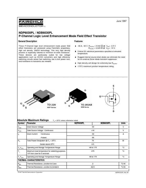
NDP6030PL / NDB6030PL P-Channel Logic Level Enhancement Mode Field Effect Transistor
General Description
These P-Channel logic level enhancement mode power field effect transistors are produced using Fairchild's proprietary, high cell density, DMOS technology. This very high density process is especially tailored to minimize on-state resistance. These devices are particularly suited for low voltage applications such as DC/DC converters and high efficiency switching circuits where fast switching, low in-line power loss, and resistance to transients are needed.
Features
-30 A, -30 V. RDS(ON) = 0.042 Ω @ VGS= -4.5 V RDS(ON) = 0.025 Ω @ VGS= -10 V. Critical DC electrical parameters specified at elevated temperature. Rugged internal source-drain diode can eliminate the need for an external Zener diode transient suppressor. High density cell design for extremely low RDS(ON). 175°C maximum junction temperature...