Description
Symbol
Description
SA D[35:0]
Q[35:0] QVLD[1:0]
CK, CK KD[1:0], KD[1:0]
CQ[1:0], CQ[1:0]
R W PLL
RST ZQ ZT RCS
MZT[1:0]
Address
Read Address is registered on CK and Write Address is registered on CK.
Registered on KD and KD during Write operations.
Aligned with CQ and CQ during Read operations.
Driven high one half cycle be
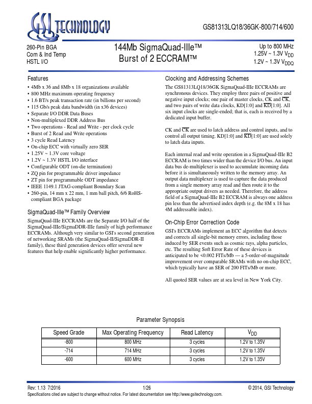
Features
- 4Mb x 36 and 8Mb x 18 organizations available.
- 800 MHz maximum operating frequency.
- 1.6 BT/s peak transaction rate (in billions per second).
- 115 Gb/s peak data bandwidth (in x36 devices).
- Separate I/O DDR Data Buses.
- Non-multiplexed DDR Address Bus.
- Two operations - Read and Write - per clock cycle.
- Burst of 2 Read and Write operations.
- 3 cycle Read Latency.
- On-chip ECC with virtually zero SER.
- 1.


