Description
Symbol
Description
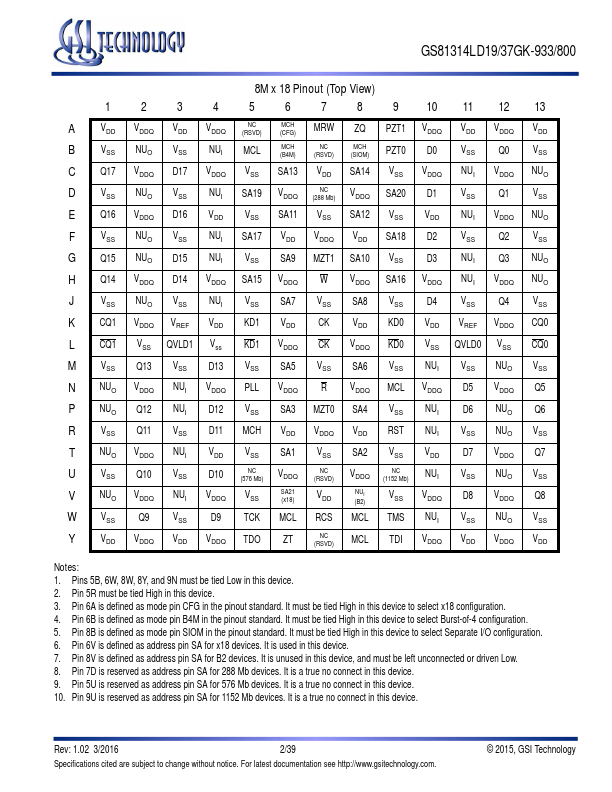
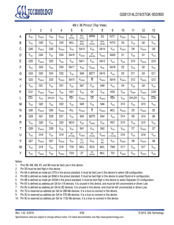
SA[21:1] D[35:0]
Q[35:0] QVLD[1:0]
CK, CK KD[1:0], KD[1:0]
CQ[1:0], CQ[1:0]
R W MRW
PLL
RST ZQ ZT RCS
Address
Read or write address is registered on CK.
Registered on KD and KD during Write operations.
Aligned with CQ and CQ during Read operations.
Driven high one half cycle before valid read data.
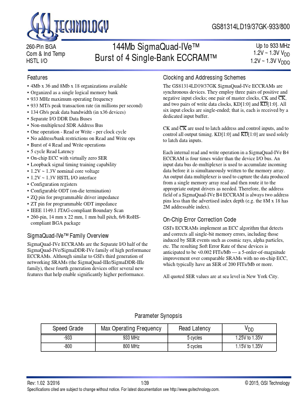
Features
- 4Mb x 36 and 8Mb x 18 organizations available.
- Organized as a single logical memory bank.
- 933 MHz maximum operating frequency.
- 933 MT/s peak transaction rate (in millions per second).
- 134 Gb/s peak data bandwidth (in x36 devices).
- Separate I/O DDR Data Buses.
- Non-multiplexed SDR Address Bus.
- One operation - Read or Write - per clock cycle.
- No address/bank restrictions on Read and Write ops.
- Burst of 4 Read.


