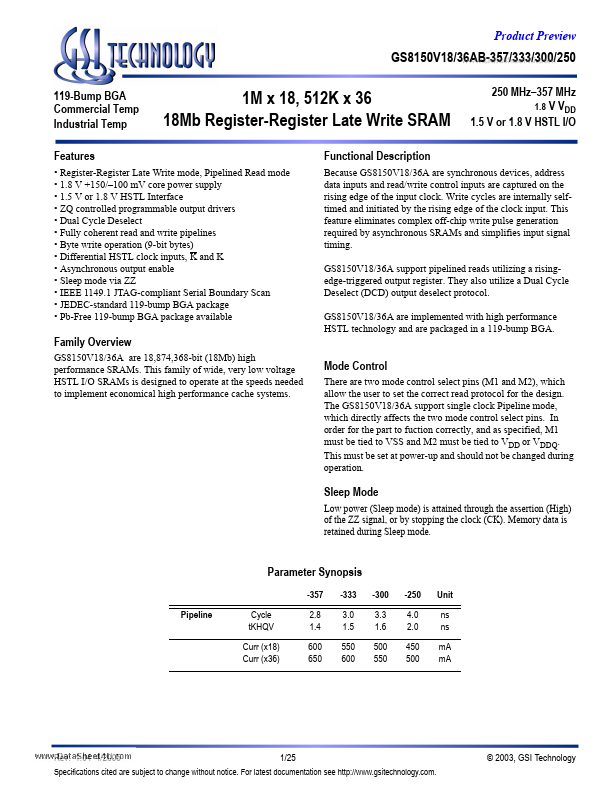
Description
250 MHz
357 MHz 1.8 V VDD 1.5 V or 1.8 V HSTL I/O
Because GS8150V18/36A are synchronous devices, address data inputs and read/write control inputs are captured on the rising edge of the input clock.Write cycles are internally selftimed and initiated by the rising edge of the clock input.This feature eliminates complex off-chip write pulse generation required by asynchronous SRAMs and simplifies input signal timing.GS8150V18/36A support pipelined reads utilizing a risingedge-triggere
Features
- Register-Register Late Write mode, Pipelined Read mode.
- 1.8 V +150/.
- 100 mV core power supply.
- 1.5 V or 1.8 V HSTL Interface.
- ZQ controlled programmable output drivers.
- Dual Cycle Deselect.
- Fully coherent read and write pipelines.
- Byte write operation (9-bit bytes).
- Differential HSTL clock inputs, K and K.
- Asynchronous output enable.
- Sleep mode via ZZ.
- IEEE 1149.1 JTAG-compliant Serial Boun.


