Description
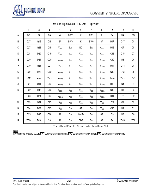
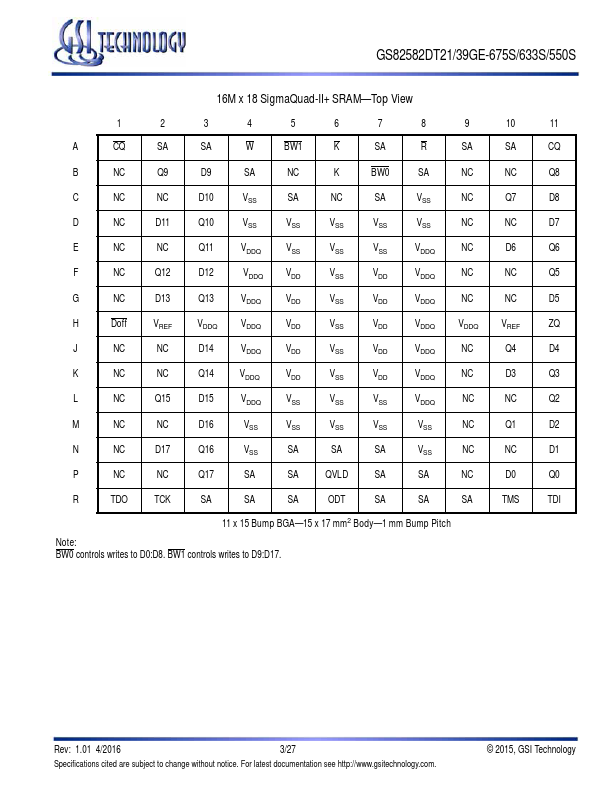
Table
Symbol
Description
Type Comments
SA Synchronous Address Inputs Input
R
Synchronous Read
Input Active Low
W
Synchronous Write
Input Active Low
BWn
Synchronous Byte Writes
Input Active Low
K
Input Clock
Input Active High
K
Input Clock
Input Active Low
Dn
Synchronous Data Inputs
Input
Qn
Synchronous Data Outputs
Output
CQ
Output Echo Clock
Output
CQ
Output Echo Clock
Output
QVLD
Q Valid Output
Output
Features
- For use with GSI FPGA-based Controller IP.
- 3.0 Clock Latency.
- Simultaneous Read and Write SigmaQuad™ Interface.
- JEDEC-standard pinout and package.
- Dual Double Data Rate interface.
- Byte Write controls sampled at data-in time.
- Burst of 4 Read and Write.
- Dual-Range On-Die Termination (ODT) on Data (D), Byte
Write (BW), and Clock (K, K) inputs.
- 1.8 V +100/.
- 100 mV core power supply.
- 1.5 V HSTL Interface.
 GS82582DT21GE-675S-GSITechnology.pdf