Datasheet Details
| Part number | HD74HC77 |
|---|---|
| Manufacturer | Hitachi Semiconductor |
| File Size | 48.25 KB |
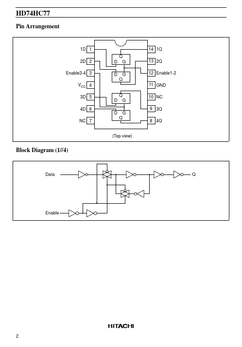
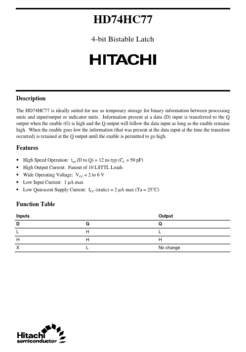
| Description | 4-bit Bistable Latch |
| Datasheet |
 HD74HC77 Datasheet HD74HC77 Datasheet
|
|
|
The HD74HC77 is ideally suited for use as temporary storage for binary information between processing units and input/output or indicator units.
| Part number | HD74HC77 |
|---|---|
| Manufacturer | Hitachi Semiconductor |
| File Size | 48.25 KB |
| Description | 4-bit Bistable Latch |
| Datasheet |
HD74HC77 Datasheet
|
|
|
|