Datasheet4U Logo Datasheet4U.com

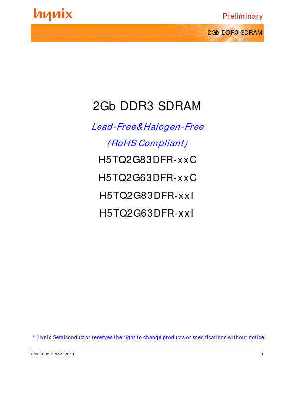
H5TQ2G83DFR-xxI, H5TQ2G83DFR-xxC Datasheet - Hynix Semiconductor

H5TQ2G83DFR-xxI - 2Gb DDR3 SDRAM

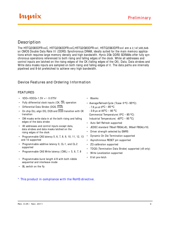
tions which requires large memory density and high bandwidth.

Hynix 2Gb DDR3 SDRAMs offer fully synchronous operations referenced to both rising and falling edges of the clock.

While all addresses and control inputs are latched on the rising edges of the CK (falling edges of the CK), Data, Data stro

H5TQ2G83DFR-xxI Features

* and Ordering Information FEATURES

* VDD=VDDQ=1.5V +/- 0.075V

* Fully differential clock inputs (CK, CK) operation

* Differential Data Strobe (DQS, DQS)

* On chip DLL align DQ, DQS and DQS transition with CK transition

* DM masks write data-in at the both risin

H5TQ2G83DFR-xxC_HynixSemiconductor.pdf

This datasheet PDF includes multiple part numbers: H5TQ2G83DFR-xxI, H5TQ2G83DFR-xxC. Please refer to the document for exact specifications by model.
H5TQ2G83DFR-xxI Datasheet Preview Page 2 H5TQ2G83DFR-xxI Datasheet Preview Page 3

Datasheet Details

Part number:

H5TQ2G83DFR-xxI, H5TQ2G83DFR-xxC

Manufacturer:

Hynix Semiconductor

File Size:

333.13 KB

Description:

2gb ddr3 sdram.

Note:

This datasheet PDF includes multiple part numbers: H5TQ2G83DFR-xxI, H5TQ2G83DFR-xxC.
Please refer to the document for exact specifications by model.

📁 Related Datasheet

📌 All Tags