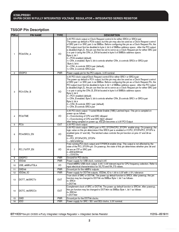
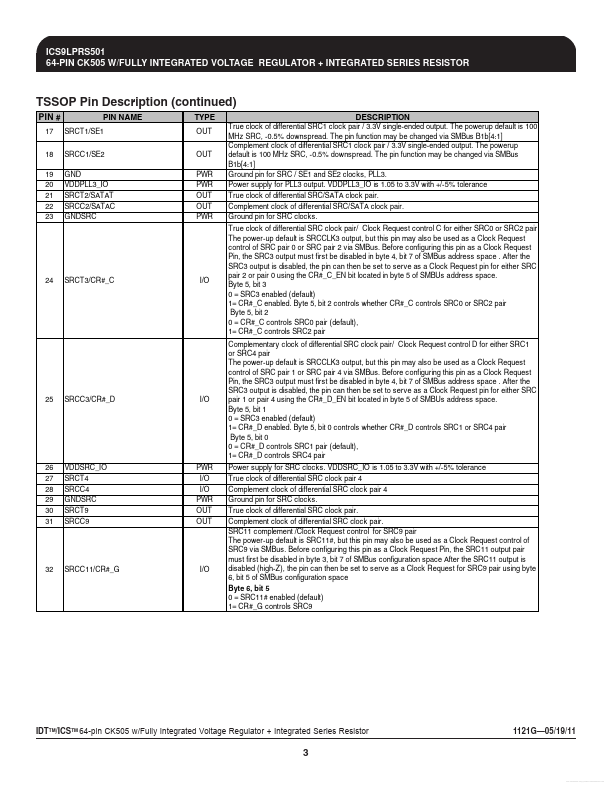
Description
PIN #
PIN NAME TYPE DESCRIPTION
3.3V PCI clock output or Clock Request control A for either SRC0 or SRC2 pair The power-up default is PCI0 output, but this pin may also be used as a Clock Request control of SRC pair 0 or SRC pair 2 via SMBus.Before configuring this pin as a Clock Request Pin, the PCI output must first be disabled in byte 2, bit 0 of SMBus address space .After the PCI output is disabled (high-Z), the pin can then be set to serve as a Clock Request pin for either SRC pair 2 or p
Features
- es/Benefits:
Does not require external pass transistor for voltage regulator Integrated series resistors on differential outputs, Zo=50Ω Supports spread spectrum modulation, default is 0.5% down spread Uses external 14.318MHz crystal, external crystal load caps are required for frequency tuning One differential push-pull pair selectable between SRC and two single-ended outputs
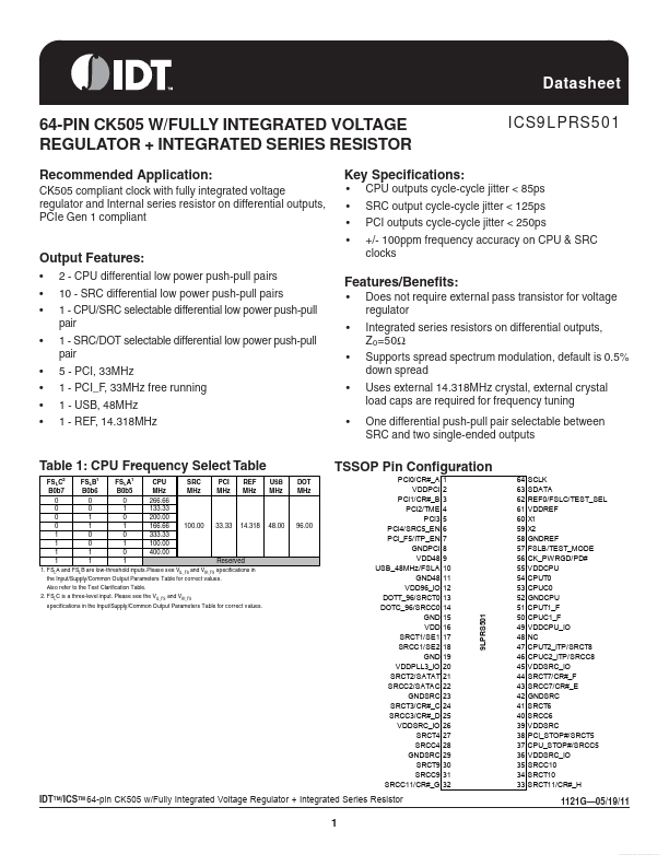
Table 1: CPU Frequency Select Table
FSLC B0b7 0 0 0 0 1 1 1 1
2
TSSOP Pin Configuration
USB MHz DOT MHz
FSLB B0b6 0 0.
 9LPRS501-IDT.pdf