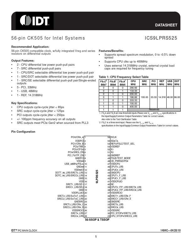
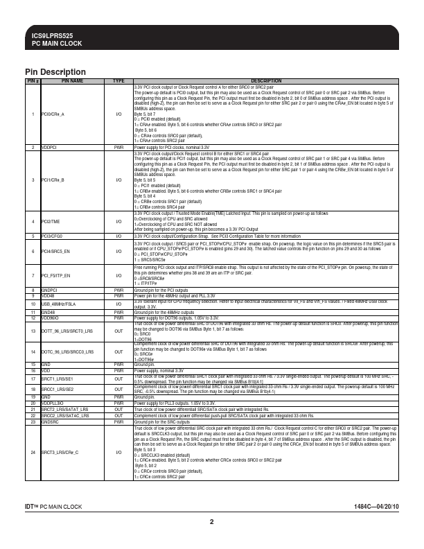
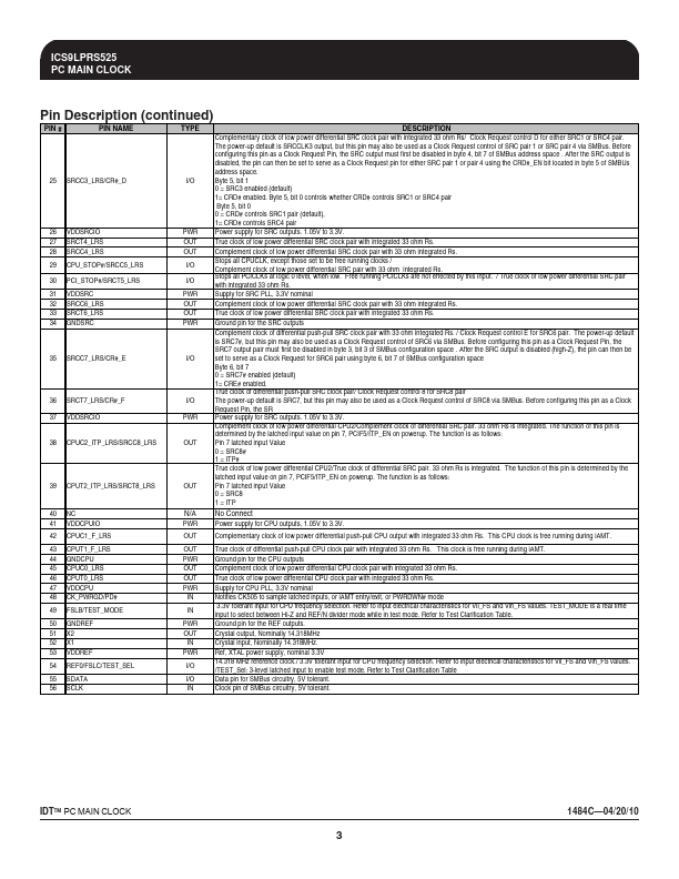
Description
PIN # PIN NAME TYPE DESCRIPTION
3.3V PCI clock output or Clock Request control A for either SRC0 or SRC2 pair The power-up default is PCI0 output, but this pin may also be used as a Clock Request control of SRC pair 0 or SRC pair 2 via SMBus.Before configuring this pin as a Clock Request Pin, the PCI output must first be disabled in byte 2, bit 0 of SMBus address space .After the PCI output is disabled (high-Z), the pin can then be set to serve as a Clock Request pin for either SRC pair 2 or p
Features
- 2 - CPU differential low power push-pull pairs.
- 7 - SRC differential push-pull pairs.
- 1 - CPU/SRC selectable differential low power push-pull pair.
- 1 - SRC/DOT selectable differential low power push-pull pair.
- 1 - SRC/SE selectable differential push-pull pair/Single-ended outputs.
- 5 - PCI, 33MHz.
- 1 - USB, 48MHz.
- 1 - REF, 14.318MHz Key Specifications:.
- CPU outputs cycle-cycle jitter < 85ps.
- SRC output cycl.
 9LPRS525-IntegratedDeviceTechnology.pdf